Do you have a question about the Harman Kardon HK 3490 and is the answer not in the manual?
| Impedance | 8 Ω |
|---|---|
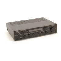
| Receiver type | Surround |
| Audio output channels | 2.1 channels |
| Total Harmonic Distortion (THD) | 0.07 % |
| Power output per channel (20-20KHz@8 Ohm) | 120 W |
| Headphone outputs | 1 |
| Headphone connectivity | - |
| Digital audio coaxial out | 0 |
| Product color | Black |
| Handheld remote control | No |
| Apple docking compatibility | Not supported |
| Connectivity technology | Wired |
| Supported radio bands | AM, FM |
| Radio Data System (RDS) | Yes |
| Preset stations quantity | 30 |
| Depth | 382 mm |
|---|---|
| Width | 440 mm |
| Height | 165 mm |
| Weight | 10400 g |
Procedure to measure leakage current to earth ground and exposed metal parts to prevent shock hazard.
Guidelines for safe servicing, including component replacement and measurements before returning the product.
List of common user-encountered problems with their potential solutions for troubleshooting.
Visual overview of the disassembly process, showing steps for removing top, front, rear panels and main PCB.
Step-by-step instructions for removing various PCBs like front panel, phone, volume, power LED, and video.
Detailed steps for removing front PCB, tuner module, video, DSP, input PCBs, power transistors, and main PCB.
Diagram showing the product disassembled into its component parts, with reference numbers.
List of electrical components with reference numbers, descriptions, and values.
List of components specific to the main PCB assembly.
Detailed list of components for the main PCB assembly.
Additional components for the main PCB assembly.
Further component listings for the main PCB assembly.
Final component listings for the main PCB assembly.
List of components specific to the input PCB assembly.
Detailed list of components for the input PCB assembly.
Additional components for the input PCB assembly.
Further component listings for the input PCB assembly.
Final component listings for the input PCB assembly.
List of components specific to the DSP PCB assembly.
Detailed list of components for the DSP PCB assembly.
Additional components for the DSP PCB assembly.
Final component listings for the DSP PCB assembly.
High-level block diagram showing the main functional blocks and their interconnections.
Diagram illustrating the internal wiring and cable connections between different circuit boards.