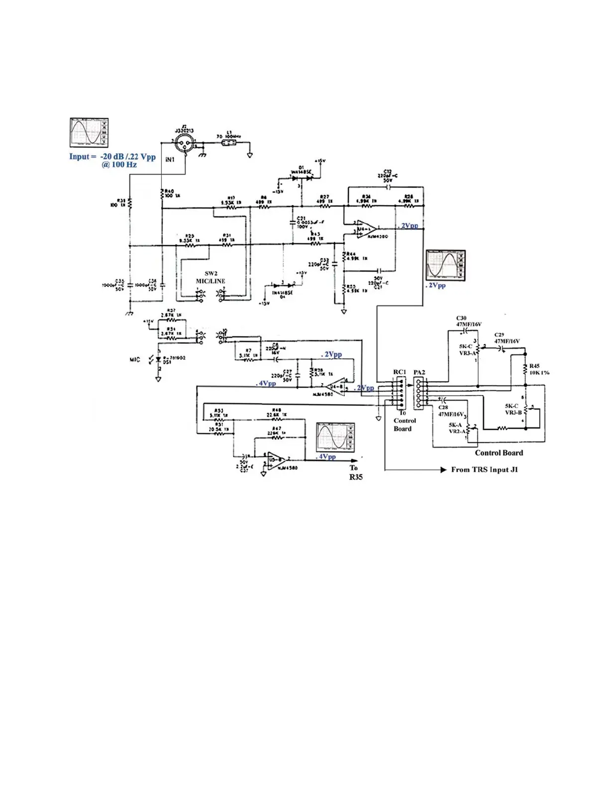
Signal Input Circuitry
The above is the XLR line input circuitry for the EON 10-G2. The balanced signal from
pins 2,3 of J2 is attenuated by R40 and R39. Signal overload is contained by the signal-
limiting diodes, D4 and D1, preventing possible internal IC damage by clamping them to the
±15 Vdc supplies. This will provide a maximum of 30 volts of signal voltage swing
between the inputs of isolation IC U4A. The output signal of this IC, pin 1, is passed
through connectors RC1, and PA2 to the volume control PCB. Coupling capacitors C28,
C29, and C30 prevent dc circuit interaction but allow signal throughput to VR2 and VR3.
Once the signal is returned to the input PCB at pin 3 of RC1, it enters the switchable-
gain/sensitivity IC U4B at pin 5. When the mic/line switch, SW2, is toggled from mic to
line input, resistors, R25/R17, are serially added to R31/R6, which increases the input
impedance at J2 input thereby decreasing the signal delivered to U4A. This action corrects
the level for proper signal amplification. The opposite occurs when SW2 is toggled in the
reverse direction. Output of U4B on pin 7 enters pin 6 of summing IC U5 via R51 and C37.
The output of this IC feeds the Loop/mix circuitry IC

 Loading...