----------------------------------------------------------------HMCS404C
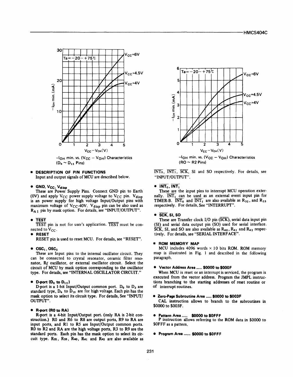
30
Ta=-20-+75"C
V
Vcc=6V
1/
J
j
......
V
V
/
.J~
Vcc=4V
Vcc=4.5V
20
I
.IV'
V
V
"
I
II
'~
~,.
J.~
i"
"
o
2 3 4
5
VCC-VOH(V)
-IOH
min.
vs.
(Vee
-
VOH)
Characteristics
(0
4
-
015 Pins)
• DESCRIPTION
OF
PIN FUNCTIONS
Input
and
output
signals
of
MCU are described below.
• GND,
Vee,
Vdisp
These are Power
Supply
Pins.
Connect
GND pin
to
Earth
(OV)
and
apply
Vee
power
supply voltage
to
Vee
pin. V
disp
is
an
power supply for high voltage
Input/Output
pins
with
maximum
voltage
of
Vee-40V.
V
disp
pin
can be also used as
RA
1 pin
by
mask
option.
For
details, see
"INPUT/OUTPUT".
•
TEST
TEST
pin
is
not
for user's application.
TEST
must
be con-
nected
to
Vee.
• RESET
RESET
pin
is
used
to
reset MCU.
For
details, see
"RESET".
•
OSC.,OSC
2
These are
Input
pins
to
the
internal oscillator circuit.
They
can be
connected
to
crystal resonator, ceramic filter reso-
nator,
Rf
oscillator,
or
external
oscillator circuit. Select
the
circuit
of
MeU
by
mask
option
corresponding
to
the
oscillator
type.
For
details, see
"INTERNAL
OSCILLATOR
CIRCUIT."
• D-port
(Do
to
0.
5
)
D-port is a
I-bit
Input/Output
common
port.
Do
to
D3
are
standard
type,
D4
to
D15
are for high voltage. Each pin has
the
mask
option
to
select its circuit
type.
For
details, See
"INPUT/
OUTPUT".
•
R-port
(RO
to
RA)
R·port
is a
4·bit
Input/Output
port.
(only
RA
is
2·bit
con·
struction.)
RO
and
R6
to
R8 are
output
ports,
R9
to
RA are
input
ports,
and
Rl
to
RS
are
Input/Output
common
ports.
RO
to
R2
and
RA
are
the
high voltage ports,
R3
to
R9
are
the
standard
ports.
Each
pin
has
the
mask
option
to
select its cir·
cuit
type. R32, R33, R40, R4.
and
R42
are also available as
6
Ta=
-20-
+75"C
5
/
V
4
J
./
V
V
~
V
J~
~
V
~
~
o
2 3
VCC-VOHeV)
/V
V
I-'
10-
V
.-
10-
I""
4
5
Vcc=6V
V
cc
=4.5V
Vee=4V
-IOH min.
vs.
(Vee
-
VOH)
Characteristics
(RO - R2 Pins)
INTo,
INT.,
SCK, SI
and
SO respectively.
For
details, see
"INPUT/OUTPUT"
.
• INTo, INT.
These are
the
input
pins
to
interrupt
MCU
operation
exter-
nally. INTI can be used as an external event
input
pin
for
TIMER-B. INTo
and
INT.
are also available as R
32
,
and
Rn
respectively.
For
details, See
"INTERRUPT".
•
SCK,SI,
SO
These are Transfer clock
I/O
pin (SCK), serial
data
input
pin
(SI)
and
serial
data
output
pin
(SO) used for serial interface.
SCK, SI,
and
SO are also available as
~o,~.
and
~2
respec-
tively.
For
details, see
"SERIAL
INTERFACE".
• ROM MEMORY MAP
MCU includes
4096
words x
10
bits ROM. ROM
memory
map
is
illustrated in Fig. I
and
described in the following
paragraph.
• Vector Address Area ..... $0000
to
$OOOF
When MCU is reset
or
an
interrupt
is serviced, the program
is
executed
from
the
vector address. Program
the
JMPL
instruc-
tions
branching
to
the
starting addresses
of
reset
routine
or
of
interrupt
routines.
• Zero-Page Subroutine Area ..... $0000
to
$003F
231
CAL
instruction
allows
to
branch
to
the
subroutines in
$0000
to
S003F.
• Pattern Area .....
$0000
to
$OFFF
P instruction allows referring
to
the ROM
data
in
$0000
to
SOFFF as a
pattern.
• Program Area ...... $0000
to
$OFFF


 To Next Page
 Loading...