HMCS404C----------------------------------------------------------------
o
15
16
63
64
4095
4096
16383
I
Vector
Address
Zero-Page Subroutine
(64Words)
Program
Pattern
(4096Words)
$0000
$oooF
$0010
\
$003F
$0040
$OFFF
$1000
$3FFF
0_
JMPL
Instruction
-
1
(Jump
to
RESET
Routine)
2_
JMPL
Instruction
-
3
(Jump
to
INTo Routine)
4
JMPL
Instruction
5-
(Jump
to
INT, Routine)
-
6
JMPL
Instruction
7 - (Jump
to
TIMER-A Routine) -
8
JMPL
Instruction
-
-
9
(Jump
to
TIMER-8 Routine)
10
11
12
JMPL
Instruction
~
-
13
(Jump
to
SERIAL Routine)
14
15
$0000
$0001
$0002
$0003
$0004
$0005
$0006
$0007
$0008
$0009
$oooA
$oooB
$OOOC
$0000
$oooE
$oooF
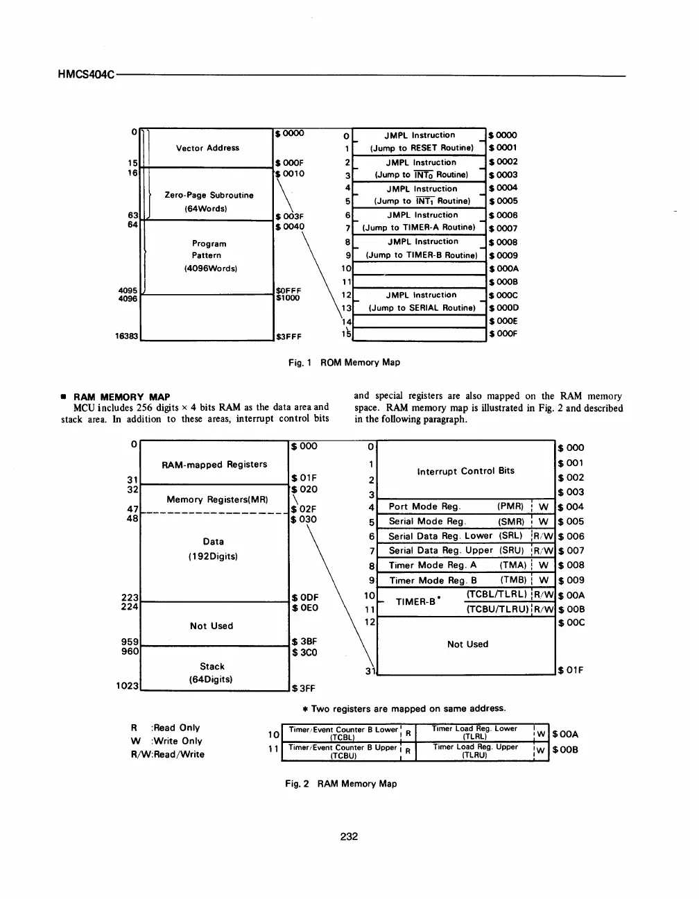
Fig. 1
ROM
Memory Map
•
RAM
MEMORY
MAP
MeV
includes 256 digits x 4 bits
RAM
as
the data area and
stack area. In addition
to
these areas, interrupt control bits
o
31
32
47
48
223
224
959
960
1023
RAM-mapped Registers
Memory
Registers(MR)
~------------------
Data
( 192Digits)
Not
Used
Stack
(64Digits)
$000
$OlF
$020
\
$ 02F
$030
$ODF
$OEO
$
3BF
$3CO
$3FF
and special registers are also mapped on the
RAM
memory
space.
RAM
memory map
is
illustrated in Fig. 2 and described
in the following paragraph.
0
1
2
3
4
5
6
7
8
9
10
~
11
12
31
Interrupt
Control
Bits
Port
Mode
Reg.
(PMR)
:W
Serial
Mode
Reg.
(SMR)
.W
Serial Data Reg.
Lower
(SRL)
!R!W
Serial Data Reg.
Upper
(SRU)
:R/W
Timer
Mode
Reg. A
(TMA)!
W
Timer
Mode
Reg. B
(TMB)
I W
TIMER-B •
(TCBLITLRL)
:RiW
(TCBUITLRU):
R/W
Not
Used
$000
$001
$002
$003
$004
$005
$006
$007
$008
$009
$OOA
$OOB
$OOC
$OlF
* Two registers are mapped on same address.
R :Read
Only
W
:Write
Only
R/W:Read/Write
Fig. 2 RAM Memory Map
232



 To Next Page