----------------------------------------------------------------HMCS404C
bit
3
bit
2
bit
1
bit
0
IMO
IFO
RSP
I/E
(1M
of
INTo)
(IF
of
INTo)
(Reset
SP
Bit)
(Interrupt
Enable Flag)
o
$000
IMTA
IFTA
IM1
IF1
(1M
of
TIMER-A)
(IF
of
TIMER-A)
(1M
of
INT
t
)
(IF
of
INT
t
)
$001
Not
Used
Not
Used
IMTB
IFTB
(1M
of
TIMER-B)
(IF
of
TIMER
-B)
2
$002
Not
Used
Not
Used
IMS
IFS
(1M
of
SERIAL) (IF
of
SERIAL)
3
$003
IF Interrupt
Aequest
Flag
1M
Interrupt
Mask
lIE
Interrupt
Enable
Flag
SP
Stack
Pointer
(Note)
Each
bit in Interrupt Control
Bits
Area
is
set
by
SEM/SEMD instruction,
is
reset
by AEM/AEMD instruction
and
is
tested
by TM/TMD
instruction.
It
is
not affected
by
other instructions. Furthermore, Interrupt
Request
Flag
is
not affected by SEM/SEMD instruction.
The
content of
Status
becomes
invarid
when
"Not
Used"
bit
is
tested.
Fig. 3
Configuration
of
Interrupt
Control
Bit
Area
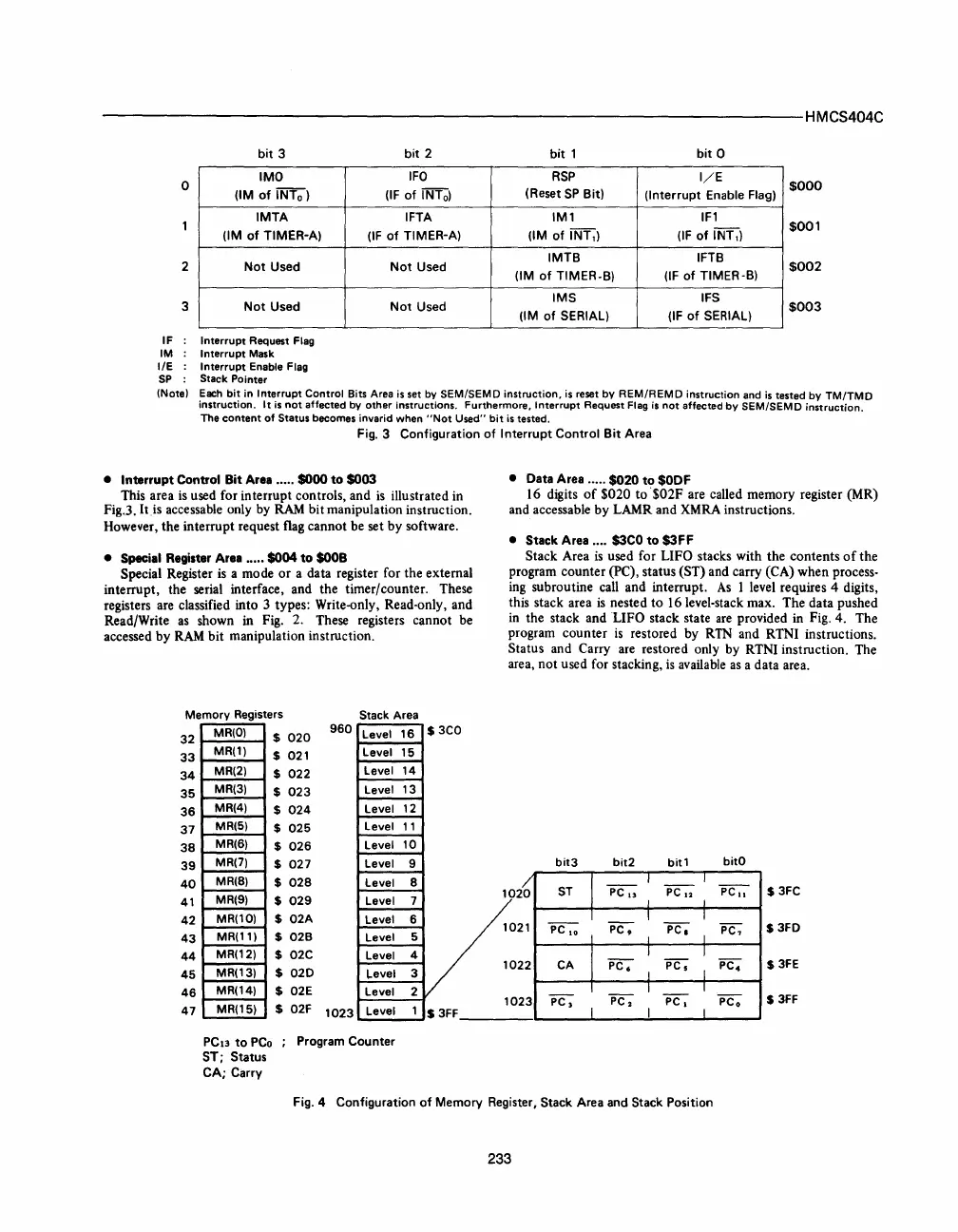
• Interrupt Control Bit Area .....
$000
to
$003
This area
is
used for interrupt controls, and
is
illustrated in
Fig.3.
It
is
accessable only by
RAM
bit manipulation instruction.
However, the interrupt request flag cannot be set
by
software.
• Special Register Area .....
$004
to
$OOB
Special Register
is
a mode
or
a data register for the external
interrupt, the serial interface, and the timer/counter. These
registers are classified into 3 types: Write-only, Read-only, and
Read/Write
as
shown in Fig. 2. These registers cannot be
accessed
by
RAM
bit manipulation instruction.
Memory Registers
Stack Area
MA(O)
$
020
960
level
16
$
3CO
MR(1)
$ 021
level
15
MR(2)
$
022
level
14
MR(3)
$
023
level
13
MR(4)
$
024
level
12
MR(5)
$
025
Level
11
MR(6)
$
026
level
10
MR(7)
$
027
level
9
MR(8)
$
028
level
8
• Data Area .....
$020
to
$ODF
16 digits
of
$020
to'$02F
are called memory register (MR)
and accessable
by
LAMR and XMRA instructions.
• Stack Area .... $lCO
to
$lFF
Stack Area
is
used for LIFO stacks with
the
contents
of
the
program counter (PC), status (ST) and carry (CA) when process-
ing subroutine call and interrupt.
As
I level requires 4 digits,
this stack area
is
nested
to
16 level-stack max. The data pushed
in the stack and
LIFO stack state are provided in Fig. 4. The
program counter
is
restored by RTN and RTNI instructions.
Status and Carry are restored only by RTNI instruction. The
area,
not
used for stacking,
is
available
as
a data area.
bitO
32
33
34
35
36
37
38
39
40
41
42
43
44
45
46
47
MR(9)
MR(10)
MR(11)
MR(12)
MR(13)
MR(14)
$
029
level
$
02A
level
$
028
level
$
02C
level
$
020
l-evel
$
02E
level
7V
6 1
5
4
3 1
2
1
PC"
$ 3FC
PC
10
PC,
$ 3FD
CA
PC"
$
3FE
~
'iiC;"
-;;-c;-
PC
o
$ 3FF
023
MR(15)
$
02F
1023
level
PCI3
to
PCo
; Program
Counter
ST;
Status
CA;
Carry
1 $ 3FF
Fig.4
Configuration
of
Memory
Register, Stack
Area
and Stack Position
233


 To Next Page
 Loading...