HMCS404C--------------------------------------------------------------
in
the Port Mode Register, the other
is
to write data into the
Serial
Mode
Register. In this state, the serial interface does not
operate although the transfer clock
is
applied.
If
STS instruc·
tion
is
executed, the serial interface changes its state
to
"SCK
waiting state".
In the "SCK waiting state", the falling edge
of
first transfer
clock affects the serial interface to get into
"transfer state",
while the Octal Counter counts·up and the Serial Data Register
shifts simultaneously.
As
an exception, if the clock continuous
output
mode
is
selected,
the
serial interface stays in "SCK wait·
ing state" while the transfer clock outputs continuously.
The
Octal Counter becomes
"000"
again by 8 transfer
clocks or execution
of
STS instruction, so
that
the serial inter·
face gets back into the "SCK waiting
state",
and SERIAL
Interrupt Request Flag
is
set simultaneojJsly.
When the internal transfer clock
is
selected, the transfer
clock
output
are triggered
by
the execution
of
STS instruction,
and it stops after 8 clocks.
• Example
of
Transfer Clock Error Detection
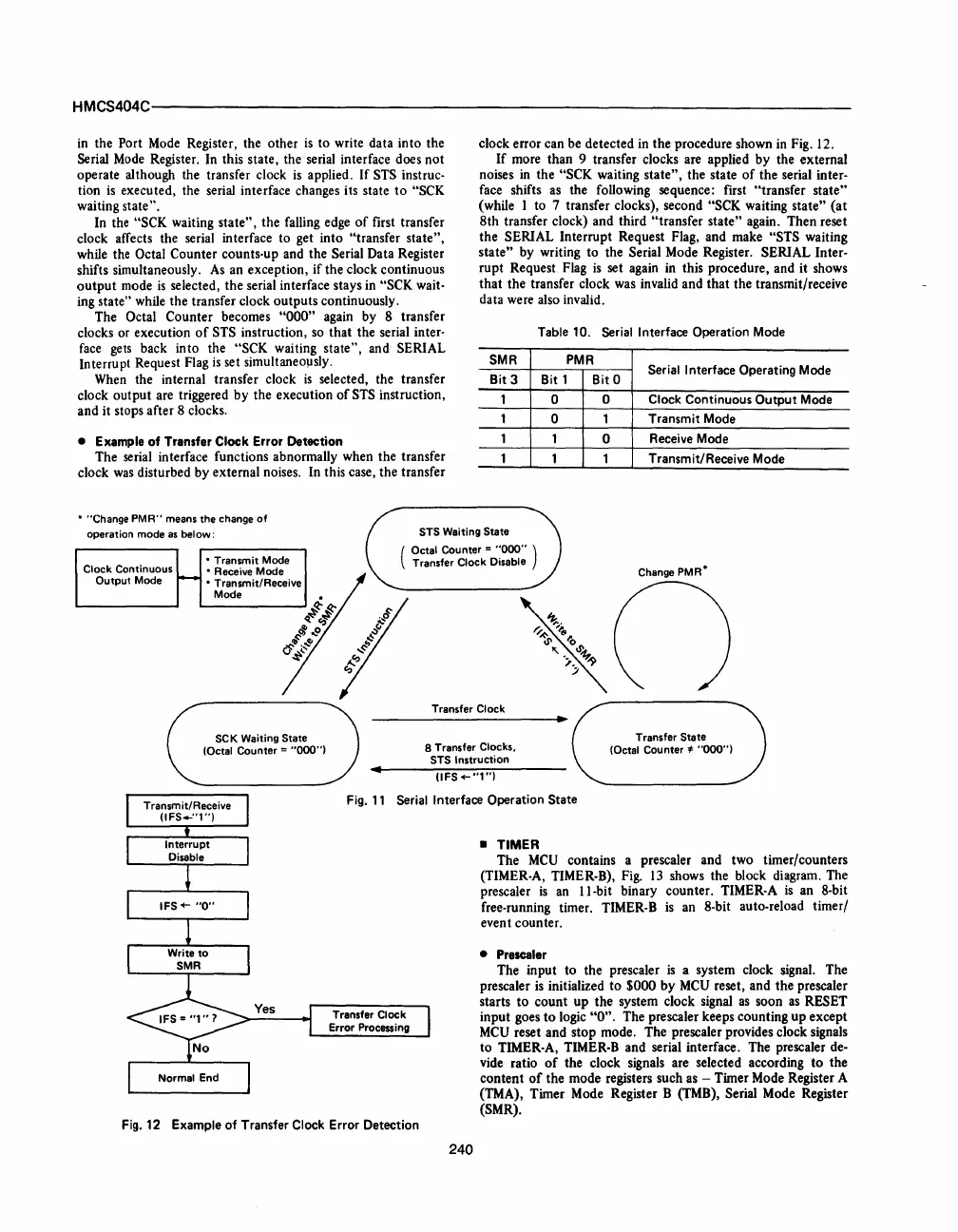
The serial interface functions abnormally when the transfer
clock
was
disturbed by external noises. In this case, the transfer
clock error can be detected in the procedure shown in Fig. 12.
If
more than 9 transfer clocks are applied
by
the external
noises in the
"SCK waiting
state",
the state
of
the serial inter·
face shifts as the fonowing sequence: first "transfer state"
(while I to 7 transfer clocks), second "SCK waiting state"
(at
8th
transfer clock) and third "transfer state" again. Then reset
the
SERIAL Interrupt Request Flag, and make "STS waiting
state"
by writing
to
the Serial Mode Register. SERIAL Inter·
rupt Request Flag
is
set again in this procedure, and it shows
that
the transfer clock was invalid and
that
the transmit/receive
data were also invalid.
Table 10. Serial Interface Operation Mode
SMR
PMR
Bit
3
Bit
1
Bit
0
Serial Interface Operating Mode
1
0
0 Clock Continuous
Output
Mode
1
0 1
Transmit Mode
1 1
0
Receive
Mode
1 1 1 Transmit/Receive Mode
• "Change
PMR"
means the change
of
operation mode
as
below:
STS Waiting State
Clock Continuous
Output Mode
t--
• Transmit Mode
• Receive Mode
• Transmit/Receive
Mode
SCK Waiting State
(Octal Counter =
"000")
(
Octal
Counter =
"000"
)
Transfer Clock Disable
Change
PMR*
Transfer Clock
8 Transfer Clocks,
STS
Instruction
(lFS
+-",")
n
Transfer State
(Octal
Counter"
"000")
Fig.
11
Serial Interface Operation State
Transfer Clock
Error
Processing
•
TIMER
The
MCU
contains a prescaler and two timer/counters
(TIMER·A, TIMER·B), Fig.
13
shows the block diagram. The
prescaler
is
an
ll-bit
binary counter. TIMER·A
is
an 8·bit
free·running
timer. TIMER·B
is
an 8·bit auto· reload timer/
event counter.
• Prescaler
The input
to
the
prescaler
is
a system clock signal. The
prescaler
is
initialized
to
$000
by
MCU
reset, and the prescaler
starts
to
count up
the
system clock signal
as
soon
as
RESET
input goes
to
logic
"0".
The prescaler keeps counting
up
except
MCU
reset and stop mode. The prescaler provides clock signals
to
TIMER·A, TIMER·B and serial interface. The prescaler de-
vide ratio
of
the clock signals are selected according
to
the
content
of
the mode registers such
as
- Timer Mode Register A
(TMA), Timer Mode Register B (TMB),
Serial Mode Register
(SMR).
Fig. 12 Example
of
Transfer Clock Error Detection
240


 To Next Page
 Loading...