EasyManua.ls Logo

Hitachi AP1 - Page 264

Hitachi AP1
378 pages
Print Icon
To Next Page IconTo Next Page
To Previous Page IconTo Previous Page
Loading...
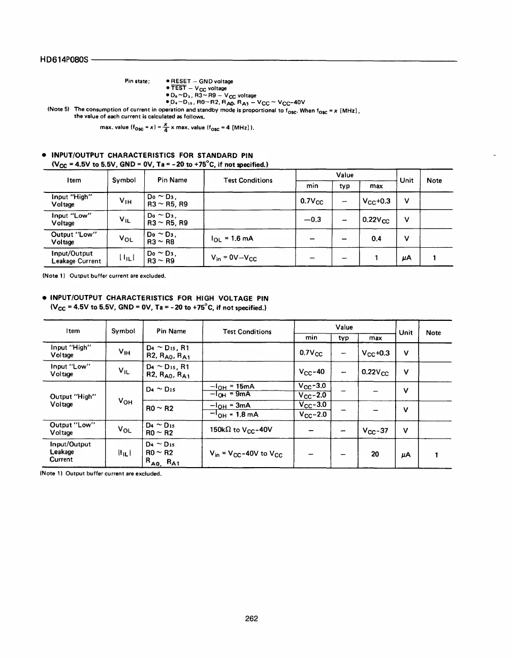
HD614P080S---------------------------------------------------------------
Pin state; - RESET -
GND
voltage
-TEST
-
Va;
voltage
-
Do
-0,.
R3 - R9 - V
cc
voltage
-.0.-
0
...
RO-R2.
RAQ.
RA1
- Vee - Vee-40V
(Note
51
The
consumption
of
current
in operation and standby mode is
proportional
to
f
osc
. When fosc = x
[MHz].
the
value
of
each
current
is
calculated
as
fOllows.
max.
value (fose = x I = T x max. value (fosc = 4
[MHz]).
• INPUT/OUTPUT CHARACTERISTICS
FOR
STANDARD PIN
(Vee = 4
5V
to
5 5V GND =
OV
Ta =
-20
to
+75°C
if
not
specified)
Item
Symbol
Pin
Name
Test Conditions
Input
"High"
VIH
Do
-
03,
Voltage
R3
-
R5,
R9
Input
"Low"
VIL
Do
- D3,
Voltage
R3-
R5,
R9
Output
"Low"
VOL
Do
-
03,
IOL = 1.6
mA
Voltage
R3-
RB
Input/Output
IIILI
Do
- D3,
Vin
=
OV-Vee
Leakage
Current
R3-
R9
(Note
11
Output
buffer
current
are excluded .
• INPUT/OUTPUT CHARACTERISTICS FOR HIGH VOLTAGE PIN
(Vee = 4.5V
to
5.5V, GND =
OV,
Ta
=
-20
to
+75°C,
if
not
specified.)
Item
Symbol
Pin
Name
Test Conditions
Input
"High"
VIH
D4
- DI5,
R1
Voltage
R2,
RAO,
RA1
Input
"Low"
VIL
04 - 015,
R1
Voltage
R2,
RAO,
RA1
D4
-
015
-lnH
= 15mA
Output
"High"
-IOH
-
9mA
Voltage
VOH
-IOH
=
3mA
RO-
R2
-I
OH
=
1.B
mA
Output
"Low"
VOL
04
-
DIS
150kil
to
Vee-4OV
Voltage
RO-
R2
Input/Output
D4
-
DIS
Leakage
IIILI
RO-
R2
Vin
=
Vee-40V
to
Vee
Current
R
AO
,
RA1
(Note
11
Output
buffer
current
are excluded.
262
Value
min
typ
0.
7V
ee
-
-0.3
-
-
-
-
-
Value
min
typ
0.
7V
ee
-
Vee-
4O
-
Vee-
3
.
O
-
Vee-
2
.
O
Vee-
3
.
O
-
Vee-
2
.
O
-
-
-
-
Unit
Note
max
Vee+
0
.
3
V
0.
22V
ee
V
0.4 V
1
p.A
1
Unit
Note
max
Vee+
0
.
3 V
0.
22V
ee
V
-
V
-
V
Ve
e
-
37
V
20
p.A
1