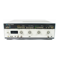
Model 214B
As can
be
seen
from
the
timing
diagram, Figure 8- 3- 2,
the
delay generator
is
similar in
function
to
the
rep. rate generator,
the
delay being determined
by
the
time
taken
to
charge the
ramp
capaci
tors
to
the
Schmitt
trigger threshold. The capacitors
are
charged via adjustable
current
source
049
/Vernier R
158,
and discharged via
current
s
witch
050,
which
switches
on
at the end
of
the
selected delay
time.
The delay generation cycle begins
on
the positive edge
of
the signal at
036
collector
(rep. rate
Schmitt
trigger) .
Transistor
s
052
/
043
turn
on
,
the
resulting positive-going voltage at
045
base
switching
04
5/
047
on
and
044
/
046
off
. (The negative edge on the
047
collector
signal
is
now
used
to
generate
the
TRIGGER
OUT
- s
ee
later
description
for
'Pulse
Po
s
ition').
Thi
s positive-going
volt
a
ge
at the
045
ba
se is
al
so
routed
to
tr
ansistor s
witch
050
,
which
turns
off,
and
allow
s
the
ramp capacitors (selected via DE
LA
Y pus
hbutton
row) to charge
from
adjustable
current
source
049
/vernier R 158.
BV
adjusting R 158, the charging
current,
and hence
time
to
reach the
Schmitt
trigger
threshold,
can
be
varied.
Upon
reaching the threshold,
046
turns on,
047
turn
s
off
, and the voltage
drop
at
the
045
base
switches
on
050
to
cause a fast discharge
of
the
ramp
capacitors.
The
delay generation cycle is
now
complete,
the
positive
edge
now
on
the
047
collector
being the start signal
for
the
width
generator.
Width Generator
The
width
generator
compri
s
es
th
e
following
functional
blocks:
- adjustable constant voltage source U 16a
- adjustable constant
current
source U
16b
/
068
/vernier
R222
- ramp capacitors
C59-C64
-
current
switch
069
-
pre-amplifier
/
Schmitt
trigger
063,
064
/
065,
066
The
width
generator
is
identical in
function
to
the delay generator,
the
width
being determined
by
the
time
taken
to
charge
the
ramp capacitors
to
the
Schmitt
trigger threshold.
The
capacitors
are
charged via
adjustable
current
source
068
/vernier R222, and discharged via
current
switch
069
which
switches on
at
the
end
of
the selected
width
time.
The
width
generation cycle begins
on
the
positive edge
of
the
signal at
047
collector
(delay
Schmitt
trigger).
Via U 1 B,
U2A
and
U3A
,
061
turns
on,
the
resulting positive-going voltage at
064
base
switching
064
/
066
on
and
063
/
065
off
.
This
positive
transition
at
064
base
is
also
routed
to
transistor
switch
069,
which
tu
r
ns
off,
and
allow
s t
he
ramp
capacitors (selected via
WIDTH
pus
hbutton
row)
to
charge
from
adjustable
current
source
068
/vernier
R222
.
By
adjusting R222,
the
charging
current
and hence
time
to
reach
the
Schmitt
trigger
thre
s
hold
, can
be
varied.
Upon reaching
the
threshold,
065
turns
on,
066
turn
s
off
, and the voltage
drop
at
the
064
b
ase
switches
on
069
to
cause a fast discharge
of
the
ramp
capacitors.
Pulse
Position
There
are
3 settings
of
th
e Pulse P
os
ition
s
witch,
the
eff
ec
t
of
ea
ch s
etting
on
the associated logic
circuit
s being de
sc
ribed in
th
e
following
paragraphs. A
simplified
functional
diagram
of
the
se
logic circ
uit
s is given in Figure 8- 3- 3.
Service
8-17
Scans by Artekmedia => 2009