Model
2148
Double
Pulse
Timing Error
With
Double
Pulse Mode selected,
the
width
generator
is
started
twice
within
a single
clock
period.
The
first
'start'
pu Ise occurs after the negative·going edge
on
the TP4 signal (i.e. delay generator
startl,
and the second start pulse after the positive-going
edge
(i.e. at the end
of
the
selected delay
period).
As
both
pulses
must
be
generated
within
one period, the
following
formula
determines valid
operation
of
the
2148:
delay + (2 x
width)
+ pulse separation
';;;
pulse period
T~~
DELAY
U
lOl11
WIOTH
U
lOl1
0
II
II
II
U619
,
II
RATE
I
--11--
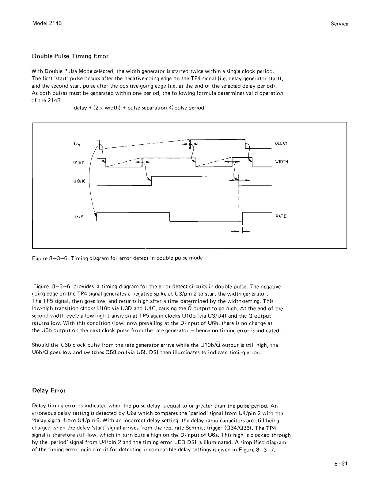
Figure 8- 3- 6.
Timing
diagram
for
error
detect
in
double
pulse mode
Figure 8- 3- 6 provides a
timing
diagram
for
the
error
detect
circuits
in
double
pulse.
The
negative·
going edge
on
the TP4 signal generates a negative spike
at
U3
/
pin
2
to
start
the
width
generator.
The
TP5
signal,
then
goes
low,
and returns high
after
a
time
det~mined
by
the
width-setting
.
This
low·high
transition
clocks U10b via
U3D
and U4C, causing the 0
output
to
go
high.
At
the end
of
the
second
width
cycle a low-high
transition
at
TP5
again clocks
U10b
(via
U3
/U4) and the Q
output
returns
low.
With
this
condition
(low)
now
prevailing at the
D-input
of
U6b,
there
is
no change
at
the
U6b
output
on
the
next
clock pulse
from
the rate generator - hence no
timing
error
is
indicated.
Should
the
U6b
clock
pu
ls
e
from
the
rate generator arrive
while
the
U10b
/Q
output
is
still
high,
the
U6b/Q goes
low
and switches
058
on
(via
U5).
DSI then illuminates
to
indicate
timing
error.
Delay Error
Delay
timing
error
is
indicated when
the
pulse delay
is
equal
to
or
greater than the pu
Ise
period.
An
erroneous delay setting
is
detected
by
U6a
which
compares the
'period'
signal
from
U4
/
pin
2
with
the
'delay signal
from
U4
/
pin
6.
With
an
incorrect
delay setting, the delay
ramp
capacitors are
still
being
charged when
the
delay
'start'
signal arrives
from
the rep. rate
Schmitt
trigger
(034
/
036).
The
TP4
signal
is
therefore
still
low,
which
in
turn
puts a high
on
the
D-input
of
U6a. This high
is
clocked
through
by
the
'period'
signal
from
U4
/
pin
2 and
the
timing
error
LED DSI
is
illuminated.
A
simplified
diagram
of
the
timing
error
logic
circuit
for
detecting
incompatible
delay settings
is
given in Figure
8-3-7.
Service
8-21
Scans by Artekmedia => 2009