Model 34SSA
THEORY OF OPERATION
Section
VIII
measurement is made to correct for
offsets. The second
measurement is made to conect for any difference
between
the plus and minus "run-down”
current references.
8-44.
Circuit Description.
8-45.
Offset Error
Measurement. Figure
8-18 shows
a
simplified schematic of the A/D
Converter. During the
offset
error
measurement all
input switches to the inte-
grator are opened. During the integration period, the
inte-
grator
is permitted to charge to a
voltage equal to any off-
set current
present
in
the integrator circuit. At the end of
the integration period the integrator
is
"run-down” and
the offset digitized and stored as the A/D Converter offset
error
by
the
main
controller.
8-46.
Current
Ratio Measurement.
During the current
ratio
measurement the plus and
minus references
are
applied to the input of the
integrator through
diode switch
Uld and U2d. The
references are
switched at
a
1 milli-
second rate
during the integration
period (133 milli-
seconds). At
the end of the integration
period, the accumu-
lated
charge on the integrator is
“run-down” digitized and
stored
as the current ratio
constant. The purpose of this
measurement is to correct
for
any
imbalance
between the
positive
and
negative current references.
8-47. TRUE
RMS AC
CONVERTER.
848. General.
8-49. The
rms
converter uses
operational circuitry, rather
than
a
thermal
element, to convert the ac signal to a
dc
level equivalent to the rms
value of the input signal. Use of
the operational rms
converter permits faster ac
measure-
ment rates. The frequency range
of the true rms converter
is 30 Hz to 1
MHz
during
normal operation and
300 Hz to
1 MHz during fast ACV
operation.
Full
scale output of the
rms converter is
6.6667
V dc.
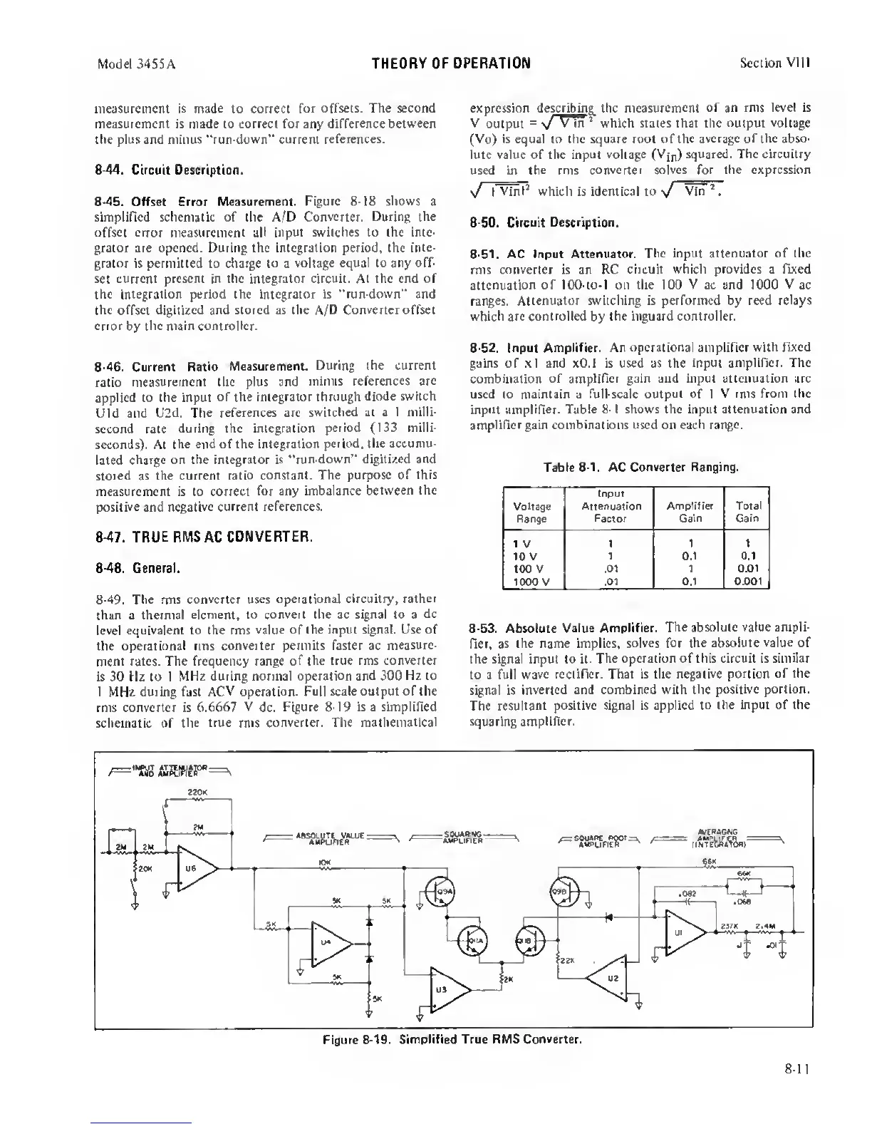
Figure
8-19
is a simplified
schematic of the true rms
converter. The
mathematical
expression describing the measurement of
an rms level is
V output
=
>/
V in
‘
which states that the output
voltage
(Vo)
is equal to the square root of the
average of the abso-
lute value of the input
voltage
(Vip)
squared. The circuitry
used in the rms
converter solves for the expression
which is identical to
8-SO. Circuit
Description.
8-51.
AC
Input Attenuator.
The Input attenuator of the
rms converter is an RC circuit
which provides a fixed
attenuation of 100-to-l on the 100 V ac and 1000
V
ac
ranges.
Attenuator switching is performed by reed relays
which
are controlled
by
the inguard controller.
8-52. Input Amplifier. An operational amplifier
with fixed
gains of xl and xO.l is used as the input
amplifier. The
combination of
amplifier gain and input attenuation are
used to maintain a full-scale output of 1
V
rms
from the
input
amplifier.
Table
8-1
shows the input attenuation and
amplifier gain combinations used on each range.
Table
8-1.
AC
Converter Ranging.
Voltage
Range
Input
Attenuation
Factor
Ampliiier
Gain
Total
Cain
1 V
1 1 1
10 V
1 0.1 0.1
100 V
.01 1
0.01
lOOOV .01 0.1
0.001
8-53.
Absolute
Value Amplifier. The
absolute value ampli-
fier, as
the name implies,
solves
for
the absolute value of
the signal input to it.
The operation of this circuit is similar
to a full
wave rectifier. That is the
negative portion of the
signal is
inverted and combined with the
positive portion.
The
resultant positive signal is applied
to
the
input of the
squaring
amplifier.
8-11
 Loading...