Section
VIII
THEORY OF
OPERATION
Model 3455A
FO
^
Mn ««0M 1
HM
j
1
nju~'Li~
1
MT«
*
CLOU
_J
1 f
mauuc
C0HtiOi,ER I
'
|i»iw iMaivt)
J
II
-
1
«*iiM
J*
™
II f
n
0*f« TMfrtrCR
eccoi
—
«
1
1
"
T
laXIRD CONmOLLCA
•
II p
n
Mm
noi
iL _rL_r
»
•«»
Figure
8-32.
Data Transfer
Signals.
Inguard controller transfer
mode, data is
valid
during
the
positive portions of the dock
signal and
changed during the
negative portions.
During the inguard
controller to main
controller
transfer mode, data is valid
during the
negative
portions
of
the clock signal and
changed during the
positive
portions. The main
controller transfers 37 bits
of informa-
tion, composed of 6 bits of trigger
information, 30 bits of
range and function
information and a parity bit, to
the
inguard controller. The inguard controller
transfers
25
bits
of information, composed of I bit of
polarity information,
23
bits of measurement data, and a
parity bit, to the main
controller.
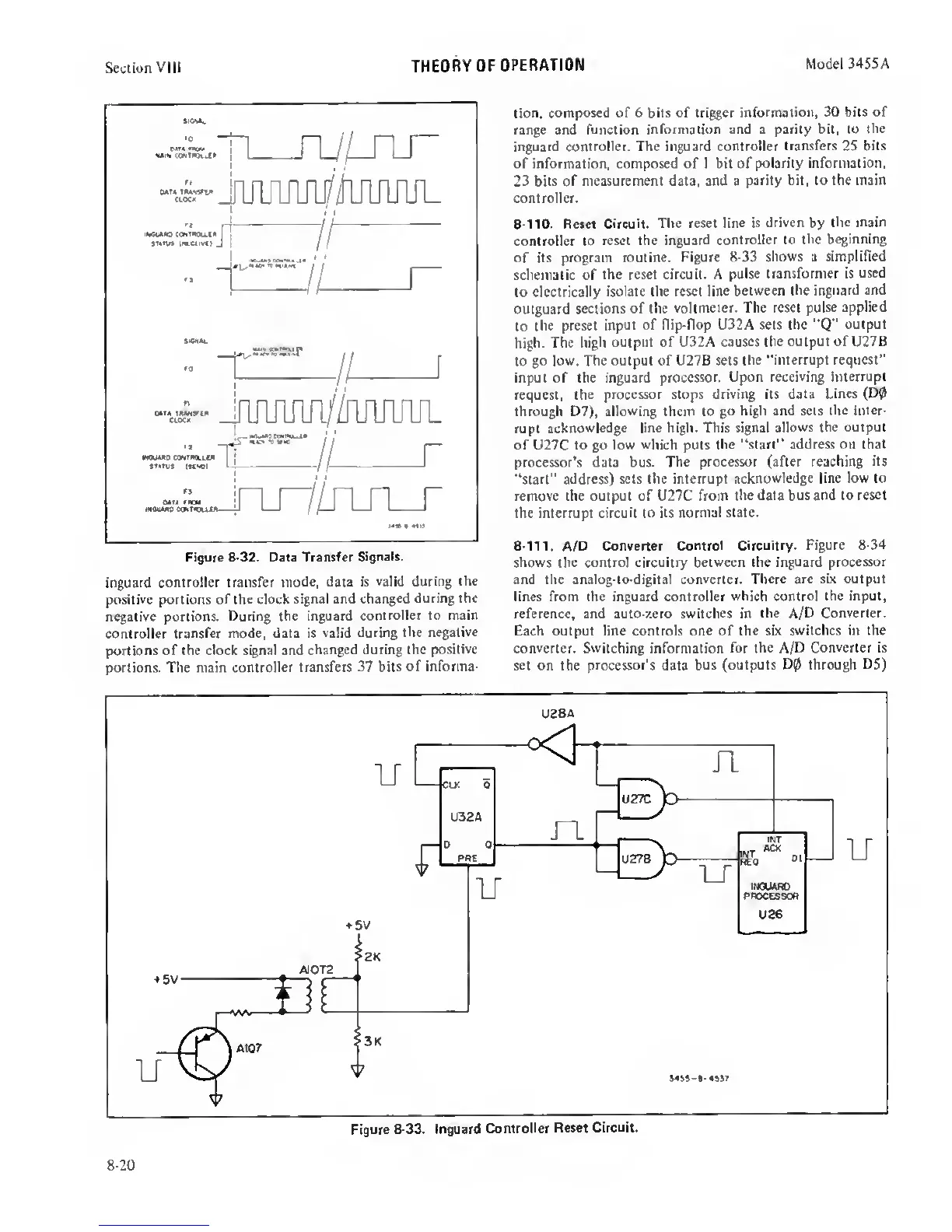
8-110.
Reset Circuit.
The reset
line
is
driven
by
the
main
controller to
reset the inguard
controller to the
beginning
of
its program routine.
Figure
8-33 shows
a
simplified
schematic of
the reset circuit. A pulse
transformer is
used
to
electrically isolate the reset
line between the
inguard and
outguard
sections of the
voltmeter. The reset
pulse applied
to
the preset
input of flip-flop U32A sets the
“Q”
output
high. The high
output of U32A causes
the output of
U276
to
go low. The output of U27B sets the
“interrupt request"
input of the inguard processor.
Upon receiving interrupt
request, the
processor stops driving its
data Lines (D0
through D7),
allowing
them to
go high and sets the
inter-
rupt
acknowledge line high. This signal
allows the output
of
U27C
to go low which puts the
“start” address on that
processor’s data bus.
The processor (after reaching
its
“start”
address) sets the interrupt
acknowledge line low to
remove the output of U27C from
the data bus and to reset
the interrupt circuit
to
its
normal state.
8-111.
A/D Converter Control
Circuitry. Figure
8-34
shows the control circuitry between the inguard
processor
and the analog-to-digital converter. There
are six output
lines from the inguard controller which
control the input,
reference, and auto-xcro switches in
the A/D Converter.
Each output fine controls
one
of the six
switches in the
converter. Switching information
for the A/D Converter is
set on the
processor's
data
bus (outputs D0 through DS)
U
28
A
Figure
8-33.
Inguard
Controller
Reset
Circuit.
8-20
 Loading...