Model 34S5A
THEORY OF OPERATION
Section VIII
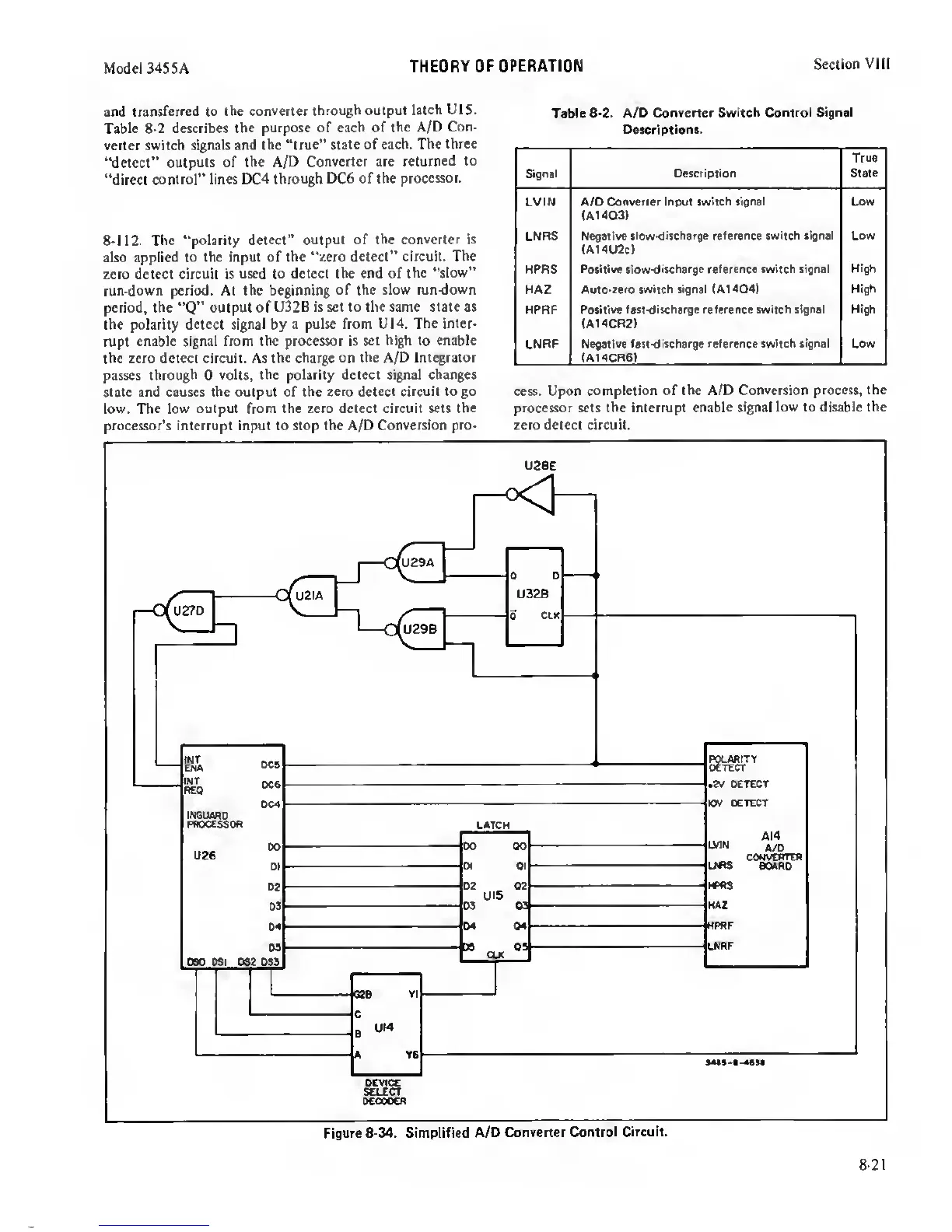
and
transferred to the converter
through output
latch UlS.
Table 8-2 describes the
purpose of each of
the A/D Con-
verter switch
signals and the “true”
state of each. The
three
“detect”
outputs of the A/D
Converter arc
returned to
“direct control”
lines DC4 through
DC6 of the
processor.
8-112. The “polarity detect”
output of the
converter is
also applied
to the input of the “:rero
detect” circuit. The
zero detect circuit is
used to detect the end of
the “slow”
run-down period. At the beginning of
the slow run-down
period, the
“Q”
output of
U32B is set to the same state as
the polarity
detect signal
by
a pulse from U14.
The inter-
rupt
enable signal from the processor is set
high
to
enable
the zero detect circuit. As the charge on
the A/D Integrator
passes
through
0
volts,
the
polarity detect signal changes
state and causes the output of the zero
detect circuit to go
low. The low
output from the zero detect circuit sets
the
processor’s interrupt input to stop the A/D
Conversion pro-
Table
6-2. A/D Converter
Switch Control Signal
DeKriptions.
Signal
Description
True
State
LVIN
A/D Convener Input
twitch signal
(A1403)
Low
LNRS Nagaiive
$low<litcharge reference switch signal
(A14U3c)
Low
Hpns
PMiiive ilow<litcherge reference switch signal
High
HAZ
Auto-zero switch signal (A14Q4)
High
HPRf
Positive fatt-diKherge reference switch signal
(A14CR2)
High
LNRF
Negative fan^iKharge reference switch signal
(A14CR6)
Low
cess. Upon
completion of the A/D
Conversion
process,
the
processor sets the interrupt
enable
signal
low
to
disable the
zero detect circuit.
Figure
8-34.
Simplified
A/O Converter
Control Circuit.
8-21