Section
Vill THEORY OF OPERATION
Model 345SA
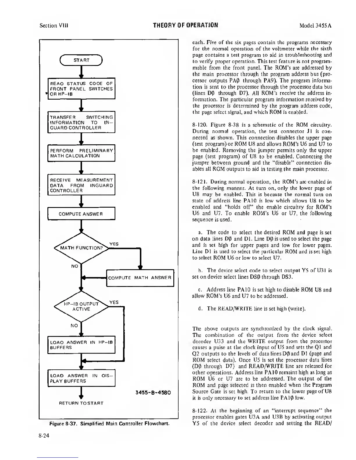
RETURN TO START
each. Five of the six pages contain the programs necessary
for
the
normal operation of the voltmeter while
the sixth
page contains
a
test program to
aid
in troubleshooting and
to verify proper operation. This test feature is not program-
mable from the front panel. The ROM’s are addressed by
the main
processor
through the program address bus (pro-
cessor outputs PA9 through PA9). The
program
informa-
tion is sent to the processor through
the
processor data bus
(lines D0 through D7).
All
ROM's receive the address in-
formation. The particular program information received by
the processor
is determined by the program address code,
the page select signal,
and
which ROM
is
enabled.
8-120.
Figure 8-38 is
a
schematic of the ROM circuitry.
During normal operation, the test connector JI
is con-
nected
as
shown.
This connection disables the upper page
(lest program) or ROM
U8
and allows
ROM’s
U6
and U7 to
be enabled. Removing
the jumper permits only the upper
page (test program) of U8
to
be enabled. Cormecting
the
jumper
between ground and the “disable" connection dis-
ables all ROM outputs
to
aid
in testing
the
main processor.
8-121.
During normal operation, the ROM's are enabled in
the following
manner. At turn on, only the lower page of
U8
may
be enabled.
This is because
the
normal turn on
state of address line PAIO is low which allows U8 to be
enabled and “holds
ofT’ the
enable
circuitry for ROM’s
U6 and U7. To enable ROM’s U6 or U7, the foUowing
sequence
is used.
a.
The code
to select the desired ROM and page is set
on data
lines D0
and Dl. Line D0 is used to select the page
and is set high
for upper pages and low for lower pages.
Line Dl is used to select the particular
ROM and is
set
high
to
select
ROM U6 or low to select U7.
b. The device select code to select output YS of
U3 1
is
sec on device select lines DS(} through DS3.
c. Address line PAIO
is
set high to disable ROM
U8 and
allow
ROM’s U6 and U7 to be addressed.
d. The READ/WRITE
line is set
high
(write).
The above outputs are synchronized by the
clock
signal.
The combination of the
output
from the
device select
decoder U33 and the
WRITE
output
from the processor
causes
a
pulse at the clock input of US and sets
the
Q 1
and
Q2
outputs to the
levels
of data
lines D<3 and Dl (page and
ROM select data). Once US is set the processor data lines
(D0 through
D7)
and
READ/WRITE line are released for
other operations. Address line PAIO remains high as long as
ROM U6 or U7 are to be addressed.
The output
of
the
ROM and page selected is then
enabled when the Program
Source Cate is
set
h^h. To
return to the lower page of U8
it is only
necessary
to
set address line PAI0 low.
Figure
8-37. Simplified Main Controller
Flowchart.
8-24
8-122.
At
the beginning of an “interrupt
sequence’’ the
processor enables gates U3A and U3B by
activating output
YS of
the device select decoder and setting the READ/
 Loading...