Model 3455A
THEORY OF
OPERATION
Section VllI
I
lacoa«
iUWnTc
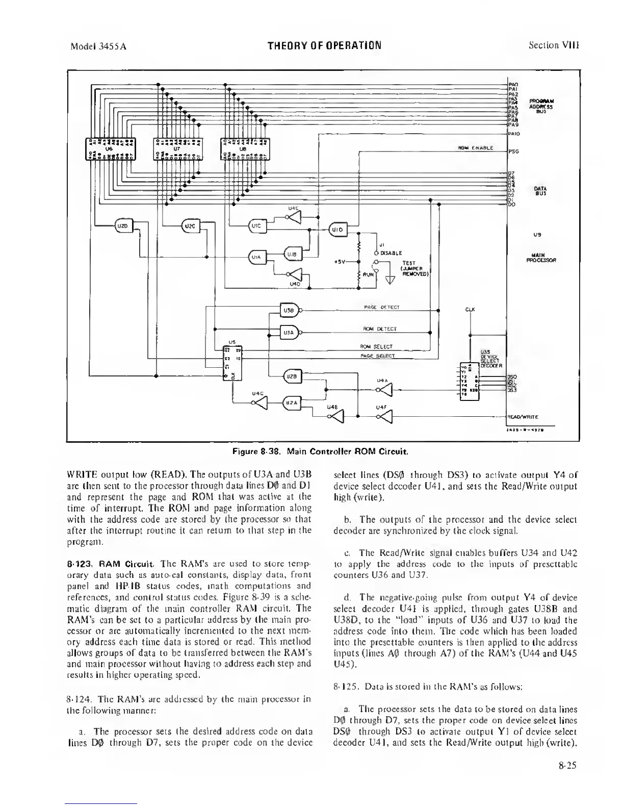
Figure 8-38. Main
Controller ROM Circuit.
WRITE output low (READ). The outputs of U3A
and U3B
are then sent to the processor
through data lines D0 and D1
and represent the page and
ROM that was
active
at the
time of interrupt. The ROM
and page information along
with the address code arc
stored
by
the processor so that
after the
interrupt routine
it can
return to that step in
the
program.
8-123. RAM Circuit. The RAM’s are used to store temp-
orary data such as auio-cal constants, display data,
front
panel and HP-IB status
codes,
math
computations and
references, and control status codes.
Figure
8-39
is a sche-
matic diagram of the main controller
RAM circuit. The
RAM's can be set to a particular
address
by
the main pro-
cessor or are automatically incremented to the next
mem-
ory address each time data is
stored or read. This method
allows groups of data to be transferred between
the
RAM's
and main processor
without having to address each step and
results in higher operating speed.
8-124.
The RAM's are addressed by the main
processor in
the following manner:
a.
The processor
sets the desired address code on data
lines
DQ) through D7. sets
the proper
code on the device
select lines (DS0 through DS3) to activate output Y4 of
device
select decoder U4I, and sets the
Read/Write
output
high (write).
b.
The outputs of the processor and the device select
decoder are synchronized by the clock signal.
c.
The
Rcad/Writc
signal enables buffers U34 and
U42
to apply the
address code
to
the
inputs of presettable
counters
U36 and U37.
d. The negative-going pulse from output Y4
of
device
select decoder U41 is applied, thix^ugh gates U38B
and
U3SD, to the "load" inputs of U36 and U37 to load
the
address code into them. The code which has been loaded
into the presettable counters
is then applied to the address
inputs (lines A0 through A7) of the RAM's (U44 and
U4S
U45).
8-I2S. Data is stored in the RAM’s
as
follows:
a. The processor sets the data to be stored
on data lines
through D7, sets the proper code on device select
lines
DS0 through
DS3
to activate
output
Y1
of device select
decoder U41, and sets the Read/Write output
high (write).
8-25
 Loading...