Section
Vni
THEORY OF
OPERATION
Model 3455A
Figure
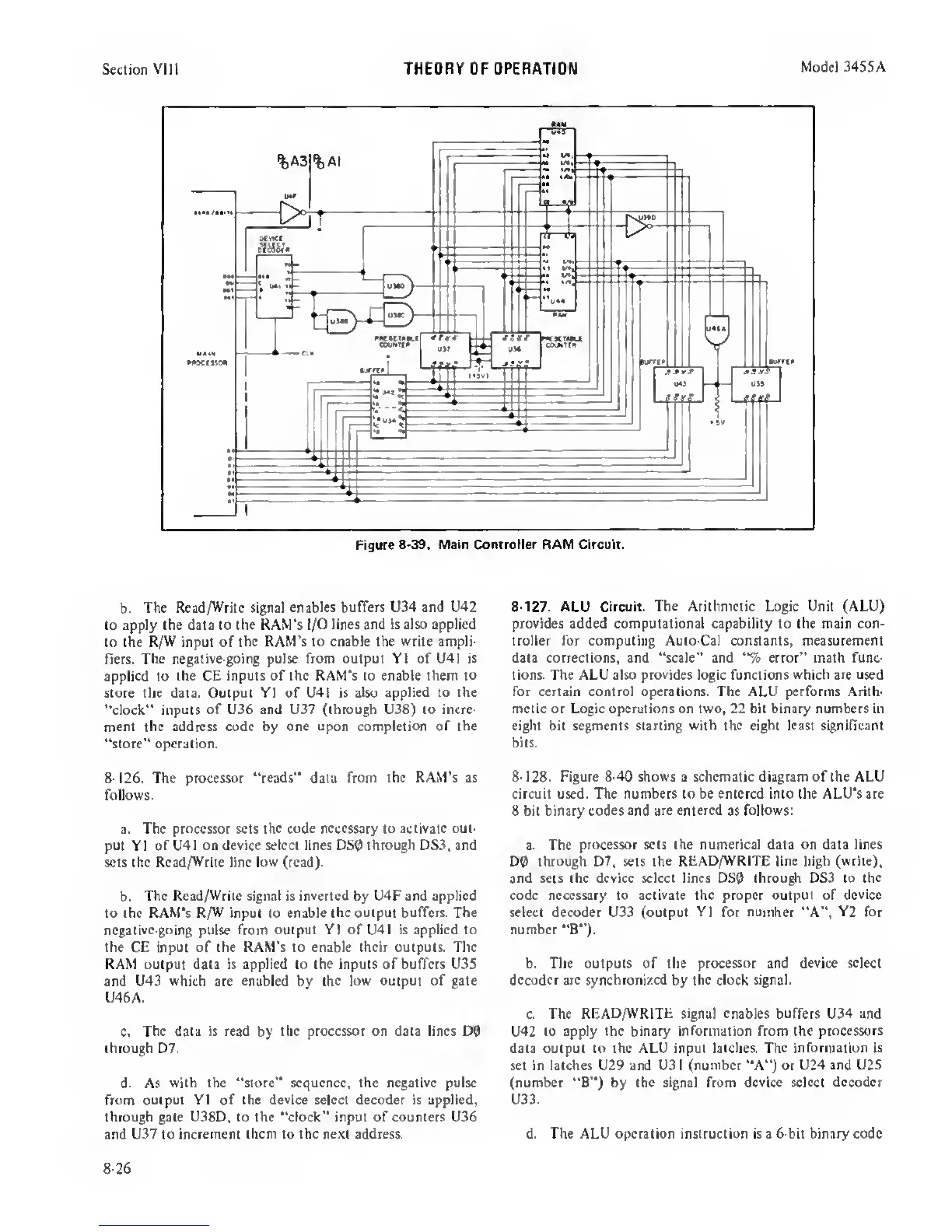
8-39. Main Controller RAM Circuit.
b.
The
Read/Writc
signal enables
buffers U34 and L)42
to apply the data to the RAM's I/O
lines and is also applied
to the
R/W
input of
the RAM's to enable the write ampli-
fiers.
The negative-going pulse from output Y1 of U41 is
applied
to
the CE inputs of the RAM’s to enable them to
store the data. Output Y1 of U4I is also
applied to the
“clock"
inputs
of
U36 and
U37
(through U38) to incre-
ment the address code by one upon completion
of
the
“store” operation.
8-126.
The processor “reads” data
from the RAM’s as
follows
a.
The processor sets the code
necessary
to
activate out-
put YI of
U4I on device select lines DS9 through DS3, and
sets the
Read/Write
line
low
(read).
b.
The Read/Write signal is inverted by U4F and applied
to the RAM's
R/W
input to enable
the
output
buffers. The
negative-going pulse from
output YI of U4I is applied to
the CE input of
the RAM's to enable their outputs. The
RAM output data is applied to the inputs of buffers U3S
and U43 which are enabled by the
low output of gate
U46A.
c.
The data
is
read
by
the processor on data lines DQ
through D7.
d. As
with the “store” sequence, the negative pulse
from output YI of the device select decoder is applied,
through gate U38D, to the “clock” input of counters U36
and U37 to
increment them
to
the next address.
8-127.
ALU
Circuit. The Arithmetic Logic Unit (ALU)
provides added computational capability to the main con-
troller for computing Auto-Cal constants, measurement
data corrections, and “scale” and
"%
error” math func-
tions. The ALU also
provides
logic functions which are used
for certain control operations. The ALU performs Arith-
metic or Logic operations on two, 22 bit binary numbers in
eight bit segments starting
with
the
eight
least significant
bits.
8-128.
Figure
8-40
shows
a
schematic diagram of the ALU
circuit used. The numbers to be entered into the ALU’s are
8 bit binary codes and are
entered
as
follows:
a. The
processor sets the numerical data on data lines
DO
through D7, sets the
READ/WRITE line high (write),
and sets the device select lines DSO through DS3 to the
code necessary to activate the proper output of
device
select decoder U33 (output YI for
number
“A”, Y2 for
number “B”).
b. The outputs of the
processor
and
device
select
decoder
arc
synchronized
by
the clock signal.
c. The
READ/WRITH
signal enables
buffers
U34 and
U42
to apply the binary information from the
processors
data output to the ALU input latches.
The information
is
set in latches U29 and U31 (number “A”) or U24 and U25
(number “B”)
by
the signal from
device select decoder
U33.
d. The ALU operation instruction is a 6-bit binary code
8-26
 Loading...