Do you have a question about the Icom IC-228A and is the answer not in the manual?
Contact information for Icom dealers or service centers for assistance.
Information required for ordering replacement parts efficiently.
Crucial safety and handling precautions for servicing the transceiver.
Covers frequency, mode, memory, power, temp, dimensions, and weight.
Details output power, modulation, deviation, emissions, and impedance.
Outlines receiver system, IF, sensitivity, selectivity, and audio output.
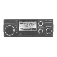
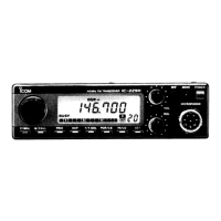
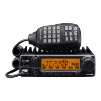
Explains the indicators and readouts on the transceiver's display.
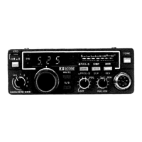
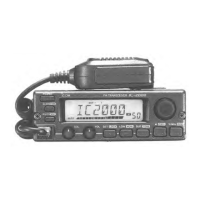
Identifies all controls, switches, and connectors on the front panel.
Identifies connectors and ports located on the rear panel.
Overall functional block diagram of the main unit.
Functional block diagram for the receiver unit.
Functional block diagram for the EF (Electronic Front) unit.
Detailed explanation of the receiver's internal circuits.
Detailed explanation of the transmitter's internal circuits.
Explanation of the Phase-Locked Loop circuits and their function.
Details CPU port allocations and key matrix for logic control.
Description and diagram of the CPU reset circuit.
Explanation of the signal strength/RF indicator circuit.
Details the display brightness control circuit.
Exploded view and steps for disassembling the front panel.
Precautions and steps before starting any maintenance or adjustment.
Step-by-step guide for adjusting the PLL circuit.
Procedures for adjusting receiver sensitivity and S-meter.
Procedures for adjusting transmitter output power and deviation.
Component and foil layouts for the EF unit.
List of all components used in the EF unit.
List of all components used in the main unit.
List of all components used in the RX unit.
Explanation of the UT-40 tone squelch unit's circuit.
Voltage and circuit diagram for the UT-40 optional unit.
Component and foil layouts for the UT-40 optional unit.
List of components for the UT-40 optional unit.
Voltage measurements for the EF and main units.
Voltage measurements for the RX unit.
| Frequency Range | 144-148 MHz |
|---|---|
| Mode | FM |
| Power Supply | 13.8 V DC |
| Dimensions | 210 x 110 x 290 mm |
| Weight | 2.6 kg |
| Antenna Impedance | 50 ohms |
| Receiver Sensitivity | 0.16 µV (12 dB SINAD) |
| Sensitivity | 0.16 µV (12 dB SINAD) |