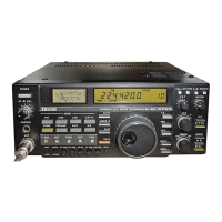
Do you have a question about the Icom IC-375A and is the answer not in the manual?
Covers frequency coverage, number of memory channels, frequency stability, power supply, current draw, dimensions, and weight.
Details emission modes, RF output power, modulation system, maximum frequency deviation, carrier suppression, unwanted sideband, and microphone impedance.
Covers receive system, receive modes, intermediate frequencies, sensitivity, squelch sensitivity, selectivity, and spurious response rejection.
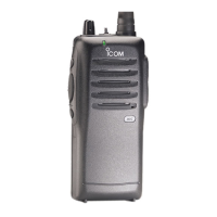
Provides diagrams of the front panel control locations and connections.
Details control locations on the front panel, including power switch, AF gain, squelch, phones jack, mic connector, and mode selectors.
Continues detailing front panel controls, including frequency display, VFO selectors, memory controls, and tuning controls.
Explains the frequency readout, data indicators, mode indicators, and other display elements.
Illustrates and labels rear panel connectors and controls, including fuse holder, power, antenna, remote control, and ground terminals.
Describes the antenna mixer circuit and noise blanker/notch filter/FM detector circuits.
Explains how RF signals are mixed with local oscillator signals for reception.
Details the noise blanker circuit, notch filter, and FM detector operation.
Explains the AF amplifier circuit, including squelch control.
Explains the FM squelch, FM S-meter, and center meter circuits.
Details the microphone amplifier circuit and the FM/SSB modulator circuit.
Explains the SSB mode circuit, including the FM modulator and SSB filter.
Details the CW mode circuit, including the key filter and SSB filter.
Describes the transmit amplifier circuitry and its connection to the antenna.
Details the Phase-Locked Loop (PLL) circuits, including the general overview and main loop.
Provides a general overview of the PLL unit, including its purpose and frequency generation.
Explains the main loop of the PLL, which controls the frequency synthesis and mixer.
Details the sub loop section, which comprises the DDS (Direct Digital Synthesizer) unit.
Explains the DDS unit, which consists of 5 ICs and generates sine wave data.
Explains how data is used for setting dividing ratios in the PLL circuits.
Covers the functions of logic circuits, including CPU, reset circuit, and matrix.
Details the CPU, its functions, and pin assignments.
Explains the reset circuit and its role in power supply and operation.
Describes the matrix table and its use for frequency step tuning and control.
Details the switching regulator circuit, which provides 13.8V DC output.
Diagram illustrating the logic and front units of the transceiver.
Diagram detailing the connector assembly for front, logic, and PLL units.
Diagram showing the main unit and RF YGR unit connector assemblies.
Instructions for disassembling the transceiver frame, including removing top and bottom covers.
Procedure for disassembling the front panel, listing components like transmit LED, switches, knobs, and buttons.
Procedure for disassembling the rear panel, including heat sink, PA unit, power sockets, and fuse holder.
Diagram showing the connector assembly for the front, logic, and PLL units.
Diagram illustrating the connector assembly for the front, main, and RF YGR units.
Diagram showing the connector assembly for the PA (Power Amplifier) and REG (Regulator) units.
Important precautions and guidelines before performing maintenance or adjustments.
Details the test instruments required and measurement connection locations for PLL adjustment.
Adjustment procedure for the DDS clock, including frequency display and receive mode.
Procedure for adjusting the 2nd LO frequency and output level.
Adjustment procedure for LPL lock voltage, including frequency display and receive mode.
Procedure for adjusting the multiplier output level, including frequency display and receive mode.
Adjustment procedure for the sub loop output, including frequency display and receive mode.
Adjustment procedure for HPL lock voltage, including frequency display and receive mode.
Details required test instruments and measurement connection locations for frequency adjustment.
Adjustment procedure for BFO frequency in different modes (LSB, CW, USB).
Adjustment procedure for PBT frequency control in different modes.
Adjustment procedure for FM frequency in FM mode.
Details test instruments and measurement connection locations for receiver adjustment.
Adjustment procedure for the FM receiver, covering various modes and controls.
Adjustment procedure for the SSB receiver, focusing on USB mode.
Procedure for adjusting the total gain of the receiver.
Adjustment procedure for the center meter in FM and other modes.
Adjustment procedure for the S-meter in USB and FM modes.
Procedure for adjusting the RF gain in USB and FM modes.
Adjustment procedure for the squelch unit.
Adjustment procedure for the noise blanker circuit.
Procedure to adjust the beep tone volume.
Details test instruments and measurement connection locations for transmitter adjustment.
Adjustment procedure for FM output power, including frequency display and transmit mode.
Procedure for adjusting output power balance in various modes.
Adjustment for the APC (Automatic Power Control) set.
Procedure for adjusting the ALC (Automatic Level Control) meter.
Adjustment for the RF meter in transmit modes.
Adjustment procedure for SWR (Standing Wave Ratio) in CW mode.
Adjustment for the compression level in USB and FM modes.
Adjustment procedure for FM drive level.
Adjustment procedure for CW drive level.
Adjustment procedure for FM deviation.
Adjustment procedure for subaudible tone.
Adjustment procedure for AQS (Automatic Quiet System) tone.
Adjustment procedure for tone squelch.
Procedure for adjusting carrier suppression in USB and LSB modes.
Adjustment procedure for transmit spurious signal levels.
Layouts for the front unit circuits, including Front (SW-A) unit and Front (SW-B) unit.
Component layout and connections for the Front (SW-A) unit.
Component layout and connections for the Front (SW-B) unit.
Component layout and connections for the Front (VR-A) unit.
Component layout and connections for the Front (VR-B) unit.
Diagrams of ICs used in the Front Unit (2), including logic and LCD driver.
Component layout on the front unit's component side.
Component layout on the front unit's foil side.
Diagrams of ICs and components for the Logic and Sensor units.
Component layout and connections for the Logic Unit.
Component layout and connections for the Sensor Unit.
Diagrams of ICs and components for the PLL and DDS units.
Component layout and connections for the PLL Unit.
Component layout and connections for the DDS Unit.
Diagrams of ICs and components for the Main Unit.
Component layout and connections for the Main Unit.
Diagrams of ICs and components for the Squelch Unit.
Component layout on the Squelch Unit's component side.
Component layout on the Squelch Unit's foil side.
Diagrams of ICs and components for the PA Unit.
Component layout and connections for the PA Unit.
Diagrams of ICs and components for the RF YGR Unit.
Component layout and connections for the RF YGR Unit.
Diagrams of ICs and components for the REG Unit.
Component layout and connections for the REG Unit.
Voltage diagram for the front unit, showing power distribution and signal paths.
Voltage diagram for the logic unit, detailing power distribution and logic signal flow.
Voltage diagram for the PLL unit, showing power distribution and signal connections.
Voltage diagram for the DDS unit, detailing power distribution and signal paths.
Voltage diagram for the main unit, showing power distribution and circuit connections.
Voltage diagrams for the regulator (REG) and power amplifier (PA) units.
Voltage diagram for the RF YGR unit, showing power distribution and circuit connections.
List of EF parts including connectors and ferrite beads with their part numbers.
List of components for the front unit, including ICs, transistors, and resistors.
Part details for Meter ME1.
List of components for the sensor unit, including ICs, transistors, and LEDs.
List of components for the logic unit, including ICs, resistors, and transistors.
List of components for the PLL unit, including ICs, FETs, transistors, diodes, and coils.
List of components for the DDS unit, including ICs, transistors, and crystals.
List of components for the main unit, including ICs, FETs, transistors, and diodes.
List of components for the Squelch unit, including ICs and transistors.
List of components for the PA unit, including ICs, transistors, and diodes.
List of components for the RF YGR unit, including ICs, transistors, diodes, and crystals.
List of components for the REG unit, including ICs, transistors, and diodes.
Schematic diagram for the front section of the IC-375A.
Schematic diagram for the sensor section of the IC-375A.
Schematic diagram for the logic section of the IC-375A.
Schematic diagram for the tone squelch section of the IC-375A.
Schematic diagram for the voice section of the IC-375A.
Schematic diagram for the main section of the IC-375A.
Schematic diagram for the regulator section of the IC-375A.
Schematic diagram for the power amplifier section of the IC-375A.
Schematic diagram for the PLL section of the IC-375A.
Schematic diagram for the EF (External Function) section of the IC-375A.
Schematic diagram for the RF YGR section of the IC-375A.
| Brand | Icom |
|---|---|
| Model | IC-375A |
| Category | Transceiver |
| Language | English |