4.1 RECEIVER
CIRCUITS
4.1.1 ANTENNA
SWITCHING
CIRCUIT
The
antenna switching circuit functions
as a
low-pass
filter
while receiving and a resonator
circuit while transmitting.
The
circuit
does not
allow transmit signals to
enter
receiver
circuits.
Received signals enter
the antenna connector
(J1)
and
pass
through
the low-pass
filter. The filtered
signals are
passed
through
the
U4
type
antenna switching circuit
(D4-D6)
and
apply
the RF
circuit.
4.1.2 RF AND 1ST MIXER
CIRCUITS
The 1st mixer circuit converts
the
received
signal
to
fixed
frequency
of the
1st
lF signal with the PLL
output frequency.
By
changing the
PLL frequency,
only the
desired
frequency
will
be
passed
through
a
pair
of crystal filters at the next
stage of
the
1st mixer.
The
signals
from
the antenna switching
circuit are
passed
through the tunable bandpass filter
(D8,
L9) and amplified
at
the
RF
amplifier
(Q1).
The
amplified signals
are again
passed
through
the tunable
bandpass
filter
(D9,
D1 1, L1 1
,
L13)
and
applied
to
the
1st mixer.
The filtered signals are mixed at the 1st mixer
(Q2)
with the 1st
LO
signal
coming from
the
Rx VCO
circuit to
produce
1st lF
signal.
The 1st lF
signal is
passed
through
the
matching
circuit
(L15,
L52) and the
pair
of crystal
filters
(Fl1).
The liltered
signal
is
amplified atthe
1st lF
amplifier
(Q4)
and applied
tothe
2nd lF circuit.
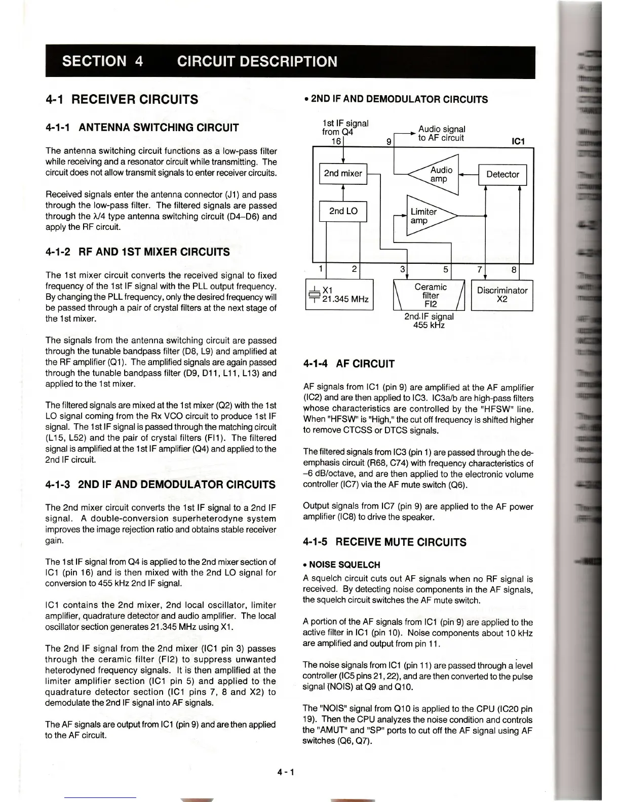
4-1.3
2ND IF AND DEMODULATOR
CIRCUITS
The 2nd mixer
circuit converts the
1st lF
signal to
a
2nd lF
signal.
A
double-conversion superheterodyne
system
improves the
image rejection ratio
and obtains stable receiver
gain.
The 1st lF signal from
Q4
is applied
to the
2nd mixer
section of
lC1
(pin
16) and
is
then mixed with the 2nd LO
signal
for
conversion to
455 kHz
2nd lF signal.
lC1 contains the
2nd mixer,
2nd local oscillator, limiter
amplifier,
quadrature
detector and audio amplifier. The local
oscillator section
generates
21.345 MHz
using
X1.
The 2nd lF signal
from
the 2nd mixer
(lC1 pin
3)
passes
through
the ceramic filter
(Fl2)
to suppress unwanted
heterodyned
frequency
signals.
lt is
then amplified
at the
limiter
amplifier
section
(lC1 pin
5) and applied to the
quadrature
detector section
(lC1 pins
7, 8 and X2) to
demodulate
the
2nd lF
signal
into AF
signals.
The AF signals are output
from
lC1
(pin
9) and are
then applied
to the AF circuit.
.
2ND lF
AND
DEMODULATOR
CIRCUITS
4-1-4
AF
CIRCU|T
AF
signals from
lC1
(pin
9)
are amplified
at the AF
amplifier
(lC2)
and
are
then applied
to lC3. lC3a/b
are high-pass
fitters
yrthose
characteristics
are controlled
by the
"HFSW"
line.
When
"HFSW"
is
"High,"
the cut
off
frequency
is
shifted higher
to
remove
CTCSS
or DTCS
signals.
The filtered
signals from
lC3
(pin
1)
are
passed
through
the de.
emphasis
circuit
(R68,
C74) with frequency
characteristics
of
-6
dB/octave,
and
are then
applied to
the electronic volume
controller
(lC7)
via
the AF mute
switch
(Q6).
Output
signals from
lC7
(pin
9) are applied
to the AF
power
amplifier
(lC8)
to drive the
speaker.
4.1-5
RECEIVE
MUTE
CIRCUITS
o
NOISE
SOUELCH
A squelch
circuit
cuts out AF
signals when
no RF
signal
is
received.
By detecting
noise
components in
the AF signals,
the
squelch circuit
switches
the AF mute
switch.
A
portion
of
the AF
signals from lCl
(pin
g)
are
apptied to the
active filter in
lC1
(pin
10).
Noise
components
about 10 kHz
are
amplified
and output from
pin
11.
The noise
signals from
lC1
(pin
1 1)
are
passed
through a ievel
controller
(f
C5
pins2l,22),
and are then
converted
to the
pulse
signal
(NOIS)
at
Q9
and
Q10.
The
"NOIS"
signal from
Q10
is
applied to the CPU
(1C20
pin
19). Then
the
CPU analyzes
the noise
condition and controls
the
"AMUT"
and
"SP"
ports
to cut off
the
AF
signal using AF
switches
(Q6,
O7).
2nd.lF
signal
455 kHz
-
4-1
-
 Loading...