4 - 7
4
5
6
7
11
12
13
14
LEDR
LEDT
LIGT
AFON
DUSE
MCON
CSFT
SPON
Outputs RX LED control signal.
Low: Lights ON.
Outputs TX LED control signal.
Low: Lights ON.
Outputs back light LED control signal.
Low: Back light is ON.
Outputs audio control signal.
Low: Outputs audio signals from
speaker.
• Outputs CTCSS/DTCS switching sig-
nal when transmitting.
High: Selected DTCS.
• Outputs Min. VR switching signal
when receiving.
Low: Select Min VR.
NOTE: Audio signals are prior to
transmitting.
Outputs microphone select signal.
High: While the internal microphone
is used.
Outputs shift signal for reference oscil-
lator’s frequency.
Outputs the internal speaker control
signal.
High: The internal speaker is select-
ed.
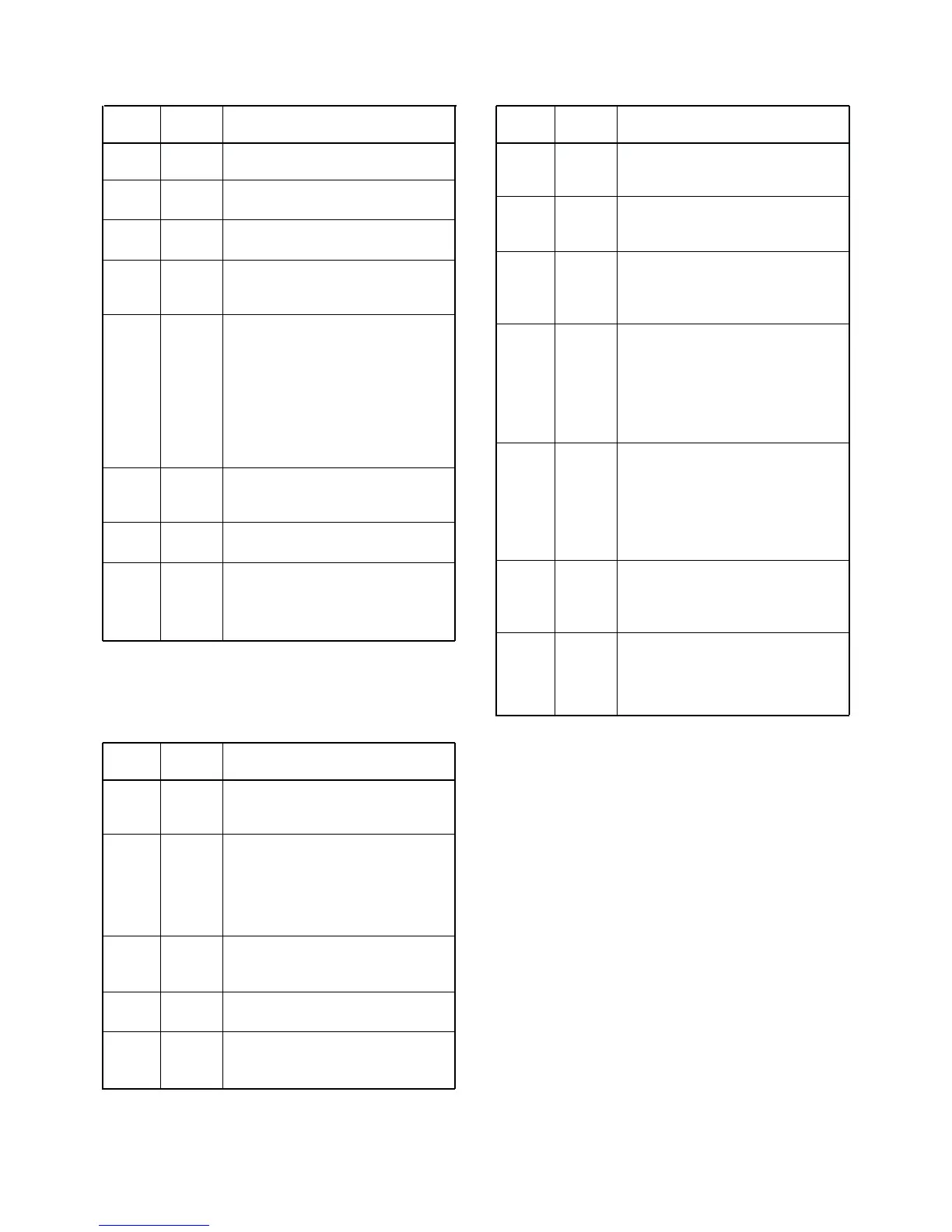
Pin Port
Description
number name
4-6-3 EXPANDER IC (FRONT UNIT; IC410)
4
5
7
11
12
13
14
R5C
T5C
S5C
MUT2
MUT1
PMFM
TMUT
Outputs the R5 regulator (Q22) control
signal.
Low: While receiving.
Outputs the T5 regulator (Q21) control
signal.
Low: While transmitting.
Outputs the S5 regulator (Q23–Q25)
control signal.
Low: While the S5 regulator outputs
5 V voltage.
Outputs the analog switch (IC13, pins
5, 6) control signal to control the
scrambler unit.
High: While the scrambler function is
ON.
Low: While the microphone mute or
AF mute is ON.
Outputs the analog switch (IC13, pins
12, 13) control signal to control the
scrambler unit.
High: While the scrambler function is
ON.
Low: While the microphone mute or
AF mute is ON.
Outputs the FM/PM modulation
switching signal to the FM/PM switch
(IC11, pin 5).
High: PM is selected.
Outputs the transmitting mute switch
control signal to the mute switch
(D38).
High: While muting.
Pin Port
Description
number name
4-6-5 EXPANDER IC (MAIN UNIT; IC12)
11
14
15
22
23
BAL
T2
T1
LVA
REF
Outputs the modulation balance level
control signal. The signal is applied to
the buffer amplifier (IC5, pin 13).
• Outputs the bandpass filter tuning
signal. The output signal is applied to
the bandpass filters (D9, D10).
• Outputs the TX power control signal.
The output signal is applied to the
APC amplifier (IC2, pin 1).
Outputs the bandpass filter tuning sig-
nal. The output signal is applied to the
bandpass filters (D3, D4, D7, D8).
Outputs the PLL lock voltage control
signal.
Outputs the reference oscillator cor-
recting voltage. The voltage is applied
to the buffer amplifier (IC5, pin 12).
Pin Port
Description
number name
4-6-4 D/A CONVERTER IC (MAIN UNIT; IC6)

 Loading...