6ED family - 2nd generation
Technical Description
Application Note 19 Rev. 1.3, 2014-03-23
AN-EICEDRIVER-6EDL04-1
The datasheet shows specific layouts, for which the given thermal resistance junction to ambient (R
th(j-a)
) is valid.
The thermal resistance which is given in the datasheet is specified for equal operation of all 6 power transistors.
It is important to know, that different layouts may lead to different thermal resistances. It is therefore always
good engineering praxis to examine additionally the package temperature by experiment.
3.9 Creepage
The clearance distance of the DSO-28 package is 1.52mm according to the package drawing. The related
parameter for TSSOP products is 0.7 mm. It depends on the individual application standard, such as [6] or [7],
as well as the application conditions, such as pollution degree, etc. to identify the relevant requirements for the
system.
The mentioned standards and similar ones describe in detail the relevant considerations for an appropriate
calculation of the creepage distance for the target system.
3.10 Layout considerations
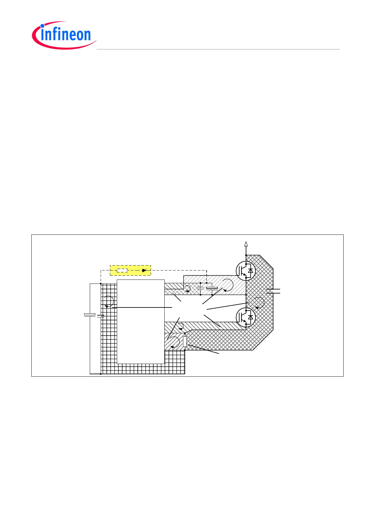
Parasitic in inductances the ground circuit or in the gate circuits exist by means of PCB track loops. They can
lead to oscillations in the according tracks. This can be the root cause of unnormal function of the IC. Figure 14
shows these inductances and track loops.
VDC
D
BS
3 x 600V / 1A
VCC
Low
inductive
shunt
Small and
short loops
LOx
HOx
VSx
COM
VSS
VBx
R
Lim
R
Sh
C
BS
C
DC
Figure 14 Parasitic inductances in the layout
First of all, the gate tracks, which connect the pins HOx and LOx with the according gate terminal of the power
transistor and the tracks connecting the emitter / source terminals of the power transistor with the VSx or COM
of the IC must be as short as possible. The area of these tracks must be minimized. This ensures, that the
switching speed of the high side transistor and the low side transistor are similar or even equal. The loop, which
consists of pin COM, the shunt resistor and pin VSS should be as well minimized. Figure 14 shows the case of
a single shunt design. Some systems may use one shunt in each phase of the drive, which is located between
source / emitter of the low side transistor and the pin COM. The pin COM and pin VSS are shorted in these
cases. The driver IC is usually stabilized by means of a low impedance capacitor, which may be a ceramic type.
The loop between pin VCC, the capacitor and VSS should also be as small as possible. This helps to minimize
the gate circuit inductances as well as the bootstrap circuit inductances. Figure 14 shows with dashed lines an
optional bootstrap circuit, which is mandatory for 6ED003L06-F2 and 6ED003L02-F2. All other types have an
integrated bootstrap diode. However, the minimization of this loop is nevertheless important.
 Loading...