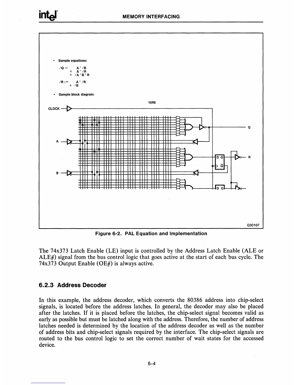
Sample equations:
10
~
A'
IB
+
A'
IR
+
IA'B'R
IR:~
A'
IR
+
IB
Sample block diagram:
CLOCK
-I>
A
--t:r-:
B
MEMORY INTERFACING
16R6
~
r--...
J
~
i-"
"
1
....
a
~--....
fll~
~~
~
....
R
oat-
~
G30107
Figure
6-2.
PAL
Equation and Implementation
The 74x373 Latch Enable (LE) input
is
controlled
by
the Address Latch Enable (ALE or
ALE#) signal from the bus control logic that
goes
active at the start of each bus cycle. The
74x373 Output Enable
(OE#)
is
always active.
6.2.3 Address Decoder
In this example, the address decoder, which converts the 80386 address into chip-select
signals,
is
located before the address latches. In general, the decoder may also be placed
after the latches.
If
it
is
placed before the latches, the chip-select signal becomes valid
as
early
as
possible but must be latched along with the address. Therefore, the number of address
latches needed
is
determined by the location of the address decoder
as
well
as
the number
of address bits and chip-select signals required
by
the interface. The chip-select signals are
routed to the bus control logic to set the correct number of wait states for the accessed
device.
6-4