MEMORY INTERFACING
6.3.3.1 3-CLK
DRAM
CONTROLLER
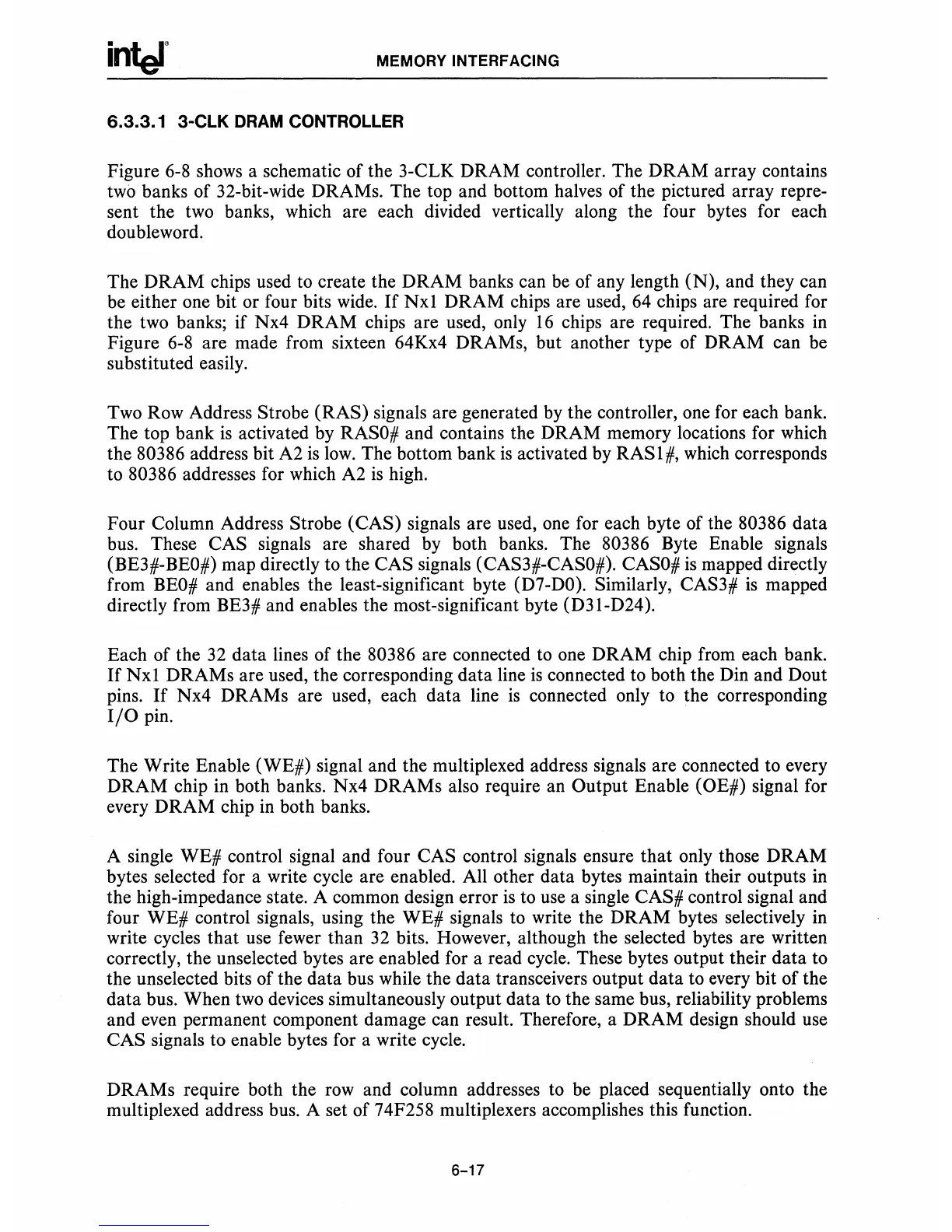
Figure 6-8 shows a schematic of the 3-CLK DRAM controller. The
DRAM
array contains
two banks of 32-bit-wide DRAMs. The top and bottom halves of the pictured array repre-
sent the two banks, which are each divided vertically along the four bytes for each
doubleword.
The
DRAM
chips used to create the
DRAM
banks can
be
of any length (N), and they can
be either one bit or four bits wide.
If
Nx1 DRAM chips are used, 64 chips are required for
the two banks; if Nx4 DRAM chips are used, only
16
chips are required. The banks in
Figure
6-8
are made from sixteen 64Kx4 DRAMs, but another type of DRAM can be
substituted easily.
Two Row Address Strobe
(RAS) signals are generated
by
the controller, one for each bank.
The top bank
is
activated by RASO# and contains the DRAM memory locations for which
the
80386 address bit A2
is
low.
The bottom bank
is
activated by RAS1#, which corresponds
to
80386 addresses for which A2
is
high.
Four Column Address Strobe
(CAS) signals are used, one for each byte of the 80386
data
bus. These CAS signals are shared by both banks. The 80386 Byte Enable signals
(BE3#-BEO#) map directly to the
CAS signals (CAS3#-CASO#). CASO#
is
mapped directly
from
BEO#
and enables the least-significant byte (D7-DO). Similarly, CAS3#
is
mapped
directly from BE3# and enables the most-significant byte (D31-D24).
Each of the 32 data lines of the
80386 are connected to one DRAM chip from each bank.
If
Nx1 DRAMs are used, the corresponding data line
is
connected to both the Din and Dout
pins.
If
Nx4 DRAMs are used, each data line
is
connected only to the corresponding
I/0
pin.
The Write Enable (WE#) signal and the multiplexed address signals are connected to every
DRAM
chip in both banks. Nx4 DRAMs also require an Output Enable (OE#) signal for
every
DRAM
chip in both banks.
A single WE# control signal and four
CAS control signals ensure
that
only those
DRAM
bytes selected for a write cycle are enabled. All other data bytes maintain their outputs in
the high-impedance state. A common design error
is
to use a single CAS# control signal and
four WE# control signals, using the WE# signals to write the
DRAM
bytes selectively in
write cycles
that
use fewer than
32
bits. However, although the selected bytes are written
correctly, the un selected bytes are enabled for a read cycle. These bytes output their data to
the un selected bits of the data bus while the
data
transceivers output data to every bit of the
data
bus. When two devices simultaneously output data to the same bus, reliability problems
and even permanent component damage can result. Therefore, a
DRAM
design should use
CAS signals to enable bytes for a write cycle.
DRAMs
require both the row and column addresses to be placed sequentially onto the
multiplexed address bus. A set of 74F258 multiplexers accomplishes this function.
6-17