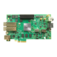
Intel Cyclone 10 GX FPGA Development Kit SDI DisplayPort HDMI
Signal V57.1 Name Signal Name Pin Number SDI FMC
Signal Name
DisplayPort
FMC Signal
Name
HDMI FMC
Signal Name
FMCA_CLK_M2
C_P1
CLK1_M2C_P CLK_M2C_P1 G2 x x x
FMCA_CLK_M2
C_N1
CLK1_M2C_N CLK_M2C_N1 G3 x x x
FMC_PRSNT PRSNT_M2C_L PRSNTN_M2C_
L
H2 x GND GND
FMC_SCL SCL SCL C30 FMC_I2C_SCL x x
FMC_SDA SDA SDA C31 FMC_I2C_SDA x x
FMC_TMS TMS JTAG_TMS D33 x x x
FMC_TDO TDO JTAG_TDO D31 x loopback Loopback
FMC_TDI TDI JTAG_TDI D30 x
FMC_TCK TCK JTAG_TCK D29 x x x
4.9.6 10/100/1000Base-T Ethernet Connector
A copper Ethernet connector (RJ1) is provided on the PCIe bracket. This interface is
implemented with Marvell 88E1111 10/100/1000Base-T Ethernet PHY.
The interface to FPGA is with SGMII through a pair of LVDS on FPGA. The PHY is
managed with MDC/MDIO management interface. The signals used and hardware
configuration pins of the Marvell device are shown in the table below:
Table 18. JTAG DIP Switch Settings
Hardware
Configuration
Pins
Connection Bits Bit [2] Bit [1] Bit [0]
Config0
GND
000
PHYADR [2:0] = 000
Config1
GND
000
ENA_PAUSE = 0 PHYADR [4:3] = 00
Config2
VDDO
111
ANEG [3:1] = 111
Config3
GND
000
ANEG [0] = 0 ENA_XC = 0 DIS_125 = 0
Config4
LED_1000
100
HWCFG_MODE [2:0] = 100
Config5
LED_10
110
DIS_FC = 1 DIS_SLEEP = 1 HWCFG_MODE [3]
= 0
Config6
LED_RX
010
SEL_TWSI = 0 INT_POL = 1 75/50 OHM = 0
The default hardware configuration is
•
Select MDC/MDIO interface. PHY address is 5'b00000.
•
INTn signal is active low
• 50 Ohm termination for SGMII
• Disable fiber/copper auto selection
4 Development Board Components
UG-20105 | 2017.12.18
Intel
®
Cyclone
®
10 GX FPGA Development Kit User Guide
37

 Loading...