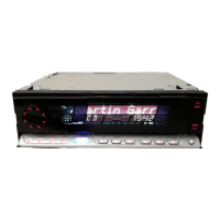
UPD789104AMC504 (IC855) : Voice control CPU
1
15
30
16
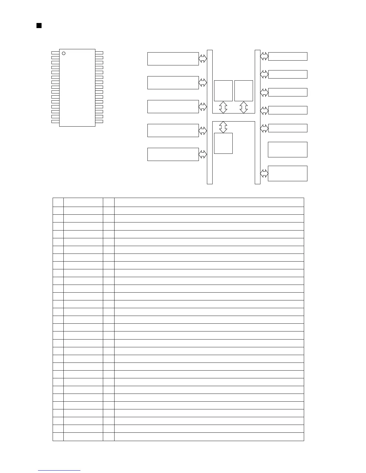
1. Pin layout
3. Pin function
2. Block diagram
PORT0
PORT1
PORT2
PORT5
PORT6
SYSTEM
CONTROL
INTERRUPT
CONTROL
8-bit TIMER/
EVENT COUNTER 80
16-bit TIMER 20
A/D CONVERTER
WATCHDOG TIMER
SERIAL
INTERFACE
RAM
ROM
78K/0S
CPU
CORE
1
2
3
4
5
6
7
8
9
10
11
12
13
14
15
16
17
18
19
20
21
22
23
24
25
26
27
28
29
30
I
I
O
-
I
I
I
I
-
-
O
I
O
O
O
O
O
O
I
-
-
-
-
-
-
O
O
I/O
O
I
J-BUS signal interruption input.
CTRL+B input H : Normal L:Power save mode.
Non connection.
Analog power supply. Connect to VDD.
Analog key input.
Non connection.
Data request input from RSC300.
When REST is H, in to the TEST mode.
Analog ground. Connect to ground.
Connect to ground.
Serial colck output for RSC300.
Data input from RSC300.
Data output for RSC300.
Mute output. L : Mute on.
Power supply control output for RSC300. H : Power supply.
Data output for RSC300.
Reset signal output for RSC300.
J-BUS I/O select output. H : Output, L : Input.
Reset detection terminal.
Connect to ground.
Connect to ground.
X'tal oscillation terminal (4.1943MHz).
X'tal oscillation terminal (4.1943MHz).
Connect to ground.
Connect to 5V.
CTRL+B output.
VOICE/CH voice select output. L : CH.
J-BUS clock input/output.
J-BUS data output.
J-BUS data input.
BUS-INT
PWR SW
NC
AVDD
KEY
NC
VREQ
TEST
AVSS
ICO
VSCK
VSI
VSO
MUTE
POWER
VENA
VRESET
BUS-I/O
RESET
ICO
ICO
X2
X1
VSS
VDD
CNT+B OUT
SELECT
BUS-SCK
BUS-SO
BUS-SI
Pin
No.
Symbol FunctionI/O
 Loading...