Do you have a question about the JVC KD-LH3101 and is the answer not in the manual?
Technical specifications for the audio amplifier components.
Technical specifications for the tuner components.
Technical specifications for the CD player components.
General technical specifications like power, dimensions, and mass.
Warnings about chassis burrs and direct beam observation.
Procedures for grounding to protect against static discharge.
Steps for disassembling the main unit of the CD receiver.
Procedure to detach the front panel assembly from the main unit.
Procedure to remove the bottom cover of the main unit.
Procedure to detach the front chassis assembly.
Procedure to remove the heat sink from the main body.
Procedure to remove the rear bracket from the main body.
Procedure to remove the main printed circuit board.
Procedure to detach the mecha control board.
Procedure to remove the CD mechanism assembly.
Procedure to remove the front board from the front panel assembly.
Procedure to remove the top cover of the CD mechanism.
Procedure to detach the connector board from the CD mechanism.
Procedure to remove the DET switch.
Procedure to remove the chassis unit from the CD mechanism.
Procedure to remove the clamper assembly.
Procedure to detach the loading/feed motor assembly.
Procedure to remove the pickup unit from the CD mechanism.
Procedure for reattaching the pickup unit.
Procedure to remove the trigger arm.
Procedure to detach the top plate assembly.
Procedure to remove the mode switch and select lock arm.
Procedure for reassembling the mode switch and select lock arm.
Procedure to detach the select arm R and link plate.
Procedure for reattaching the select arm R and link plate.
Procedure to detach the loading roller assembly.
Procedure to remove loading gears 5, 6, and 7.
Detailed procedure for removing various gears from the CD mechanism.
Procedure to detach the turntable and spindle motor assembly.
Steps and required tools for adjusting the device.
Diagnostic guide for common operational issues.
Diagram illustrating the operational flow for TOC reading.
Steps for cleaning and maintaining the laser pickup.
Step-by-step guide for replacing the laser pickup.
Pin layout and block diagram for the BA530FP-X power driver IC.
Detailed description of each pin's function for the IC.
Pin layout, block diagram, and pin functions of the voltage detector IC.
Pin layout, block diagram, and pin functions of the EEPROM IC.
Pin layout, block diagram, and pin functions of the EEPROM IC.
Pin layout and block diagram for the quad analog switch IC.
Pin layout and block diagram for the HA13164A regulator IC.
Pin layout, pin function table, and block diagram for the buffer IC.
Pin layout, pin function table, and block diagram for the buffer IC.
Pin layout and block diagram for the IC-PST3424U-X reset IC.
Pin layout and block diagram for the IC-PST9333U-X regulator IC.
Pin layout and block diagram for the M62449FP-X equalizer IC.
Block diagram for the LA47505 power amplifier IC.
Pin function details for the LA47505 power amplifier IC.
Pin layout and block diagram for the 16M flash memory IC.
Pin function details for the LH28F160BJHET92 flash memory IC.
Pin layout and pin function details for the LCD display sub CPU.
Pin function details for the MN102H60KCG LCD display sub CPU.
Pin layout and block diagram for the DC-DC converter IC.
Pin layout and block diagram for the dual operational amplifier IC.
Pin layout and block diagram for the NJU7241F25-X regulator IC.
Pin layout for the NJU7241F33-X voltage regulator IC.
Block diagram for the RPM6938-SV4 remote control receiver.
Pin layout and block diagram for the D/A converter IC.
Pin layout and block diagram for the RDS detector IC.
Pin layout and block diagram for the RF amplifier IC.
Pin function details for the TA2157FN-X RF amplifier IC.
Pin layout and block diagram for the DSP & DAC IC.
Pin function details for the TC94A14FA DSP & DAC IC.
Pin layout and block diagram for the audio digital processor IC.
Pin function details for the TC94A20F-008 audio digital processor IC.
Pin layout and block diagram for the CPU IC.
Pin function details for the TMP91CW12AF4RA3 CPU IC.
Pin layout and block diagram for the UPD784217AGC220 CPU IC.
Pin function details for the UPD784217AGC220 CPU IC.
Pin layout and block diagram for the car radio signal processor IC.
Overall block diagram of the CD receiver system.
Schematic diagram of the main amplifier circuit.
Schematic diagram of the CD servo control circuit.
Schematic diagram of the LCD and key control circuits.
Layouts for the main board and mecha control board.
Layouts for the front board and mecha control board.
Layouts for the front board and mecha control board.
Exploded view showing assembly and parts identification.
Parts list for the CD mechanism assembly.
List of electrical components used in the main board.
List of packing materials and accessories.
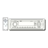
| Detachable Face | Yes |
|---|---|
| Sub Preamp Output | Yes |
| CEA-2006 Compliant | Yes |
| MP3 Playback | Yes |
| WMA Playback | Yes |
| ID3 Tag Display | Yes |
| iPod Compatibility | Yes |
| Bluetooth Compatibility | No |
| HD Radio | No |
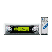
| Remote Control | Yes |
| CD Playback | Yes |
| Peak Power Output | 50 watts x 4 |
| RMS Power Bandwidth | 20 Hz - 20 kHz |
| Preamp Voltage | 2.5 volts |
| Equalizer | 3-Band |
| Tuner | FM/AM |