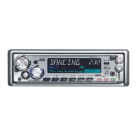
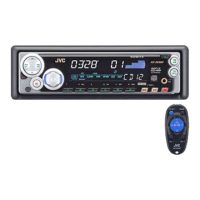
KD-SX979R/KD-SX925R
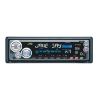
KD-SX924R/KD-SX909R
2-13
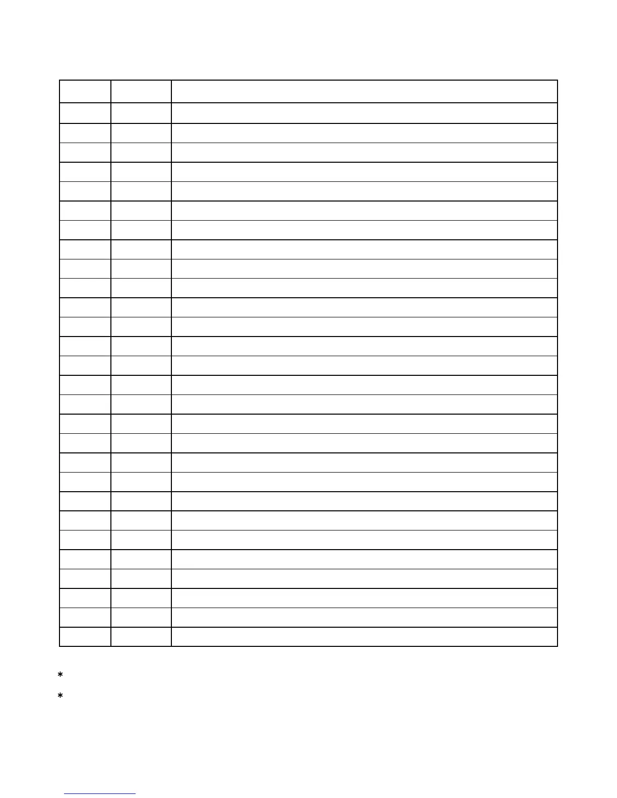
Pin NO. Symbol Function
1
2
3
4
5
6
7
8
9
10
11
12
13
14
15
16
17
18
19
20
21
22
23
24
25
26
27
28
VCC2
V05-
V05+
V04+
V04-
V03+
V03-
V02+
V02-
V01+
V01-
VCC1
VIN1+
VIN1-
VIN2+
VIN2-
VIN3+
VIN3-
REG-IN
REG-OUT
VREF-IN
VCC-S
VIN4-
VIN4+
MUTE
S-GND
FWD
REV
Power for channels 3,4, and 5 (VCC1 and VCC-S short-circuited)
Loading output (-)
Loading output (+)
Output pin (+) for channel 4
Output pin (-) for channel 4
Output pin (+) for channel 3
Output pin (-) for channel 3
Output pin (+) for channel 2
Output pin (-) for channel 2
Output pin (+) for channel 1
Output pin(-) for channel 1
Power for channels 1 and 2 (BTL), (VCC-S and VCC2 short-circuited)
Input pin for channel 1
Input pin for channel 1 (for gain control)
Input pin for channel 2
Input pin for channel 2 (for gain control)
Input pin for channel 3
Input pin for channel 3 (for gain control)
Regulator pin (External PNP base)
Regulator pin (External PNP collector)
Reference voltage input pin
Signal system power (VCC and VCC2 short-circuited)
Input pin for channel 4 (for gain control)
Input pin for channel 4
Output ON/OFF, channels 1 to 4 (BTL AMP)
Signal system GND
5CH(VL0) Output change pin (FWD), Logic input for loading block
5CH(VL0) Output change pin (REV), Logic input for loading block
The center frame (FR) functions as power system GND. Set this to the minimum potential together with S-GND.
Short-circuit three pins of power system, VCC-S, VCC1, and VCC2, externally before use.
3.Pin function
LA6557-X(2/2)
 Loading...