KS-FX230
1-13
1 to 16
48 to 33
49
64
32
17
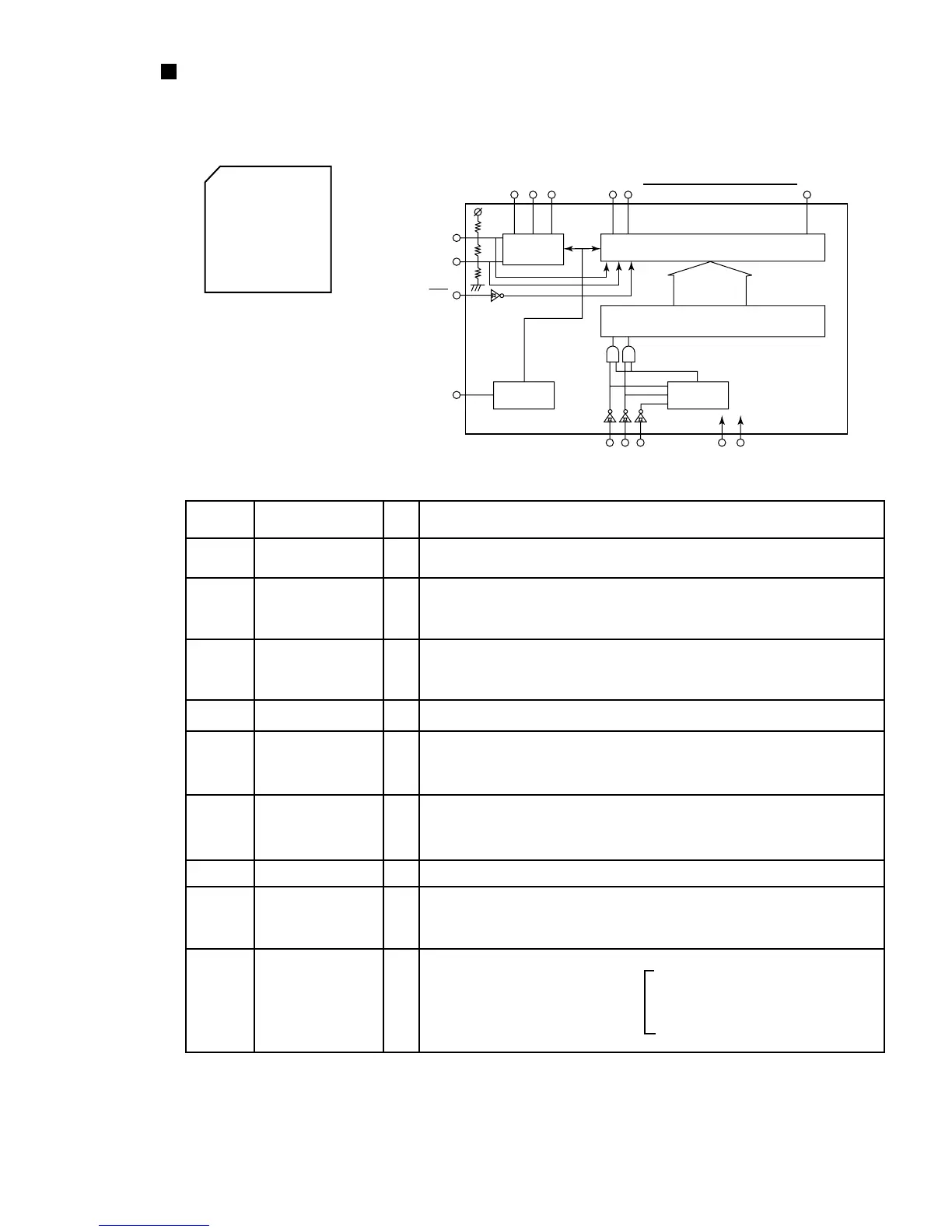
1.Pin layout
2.Block diagram
PIN
No.
1 to 9
10 to 52
53 to 55
56
57
58
59
60
61
62
63
64
S10 to S52
COM1 to COM3
VDD
/INH
VSS
OSC
CE
CL
DI
NOT USED
Segment outputs that display data transferred from
serial data.
The frame frequency (fo) for the common driver output is
(fosc/384)Hz.
Power supply
Forcibly terns off the display. regardless of internal data.
Serial data can be input. whether this pin is high or low
NOT USED
To GND
Oscillator connection (for the common segment alternating
waveform)
Serial data transfer
pins.connected to a
microprocessor.
-
O
O
-
I
-
-
-
I
I
I
I
CE : Chip enable
CL : Sync.clock
DI : Transfer data
Symbol I/O
Functions
3.Pin function
LC75823E(IC651):LCD driver
to to
COM1 COM2 COM3 S52 S51 S1
LATCH & DRIVER
SHIFT REGISTER
ADDRESS
DETECTOR
COMMON
DRIVER
CLOCK
GENERATOR
VDD1
VDD2
INH
OSC
DI CL CE
VDD VSS
 Loading...