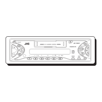
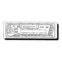
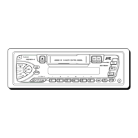
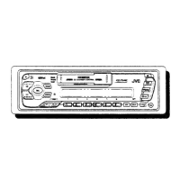
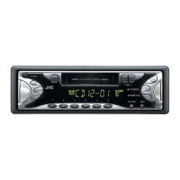
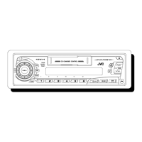
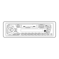
KS-FX621
(No.49825)1-27
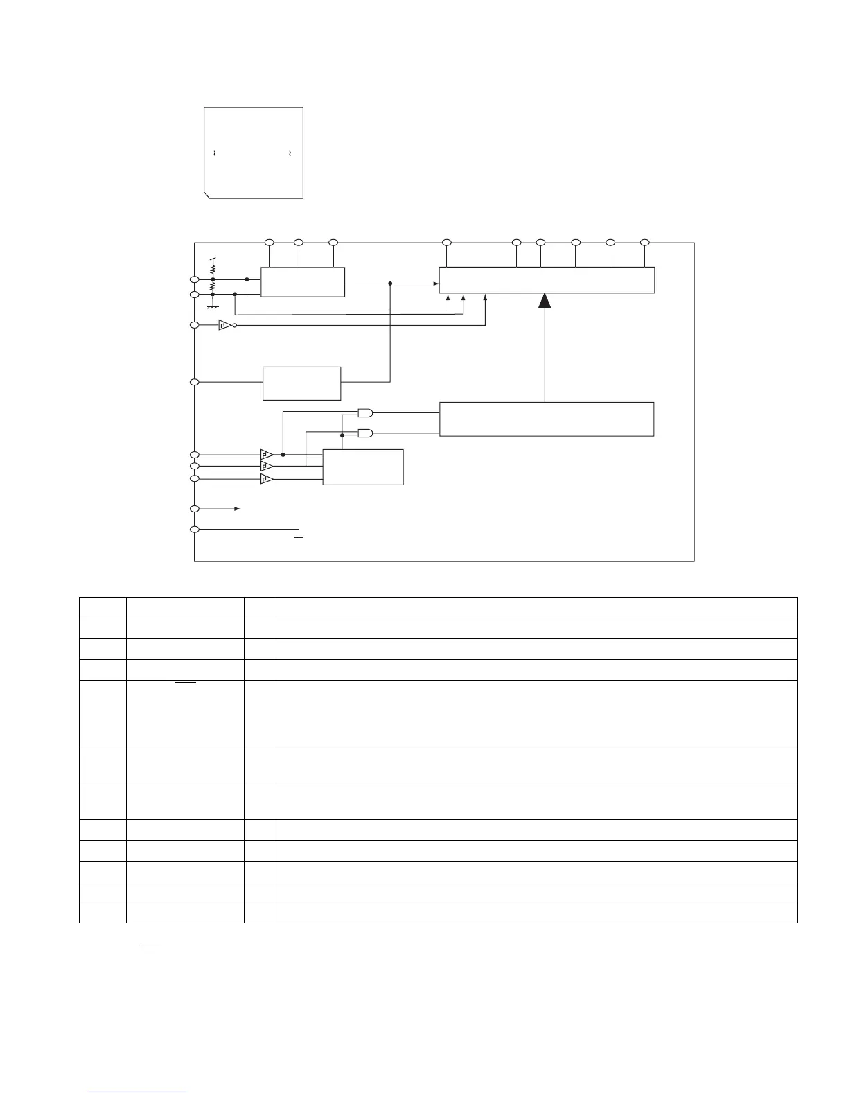
4.6 PT6523LQ (IC651) : LCD driver
•Pin layout
• Block diagram
• Piin function
Note 1:
When INH
= "LOW" : Serial data trensfers can be performed when the display is forcibly OFF.
1 ~ 16
48 ~ 33
32
17
49
64
Pin No. Pin Name I/O Description
1~ 52 SG1 ~ SG52 O Segment Output Pins
53~55 COM1 ~ COM3 O Common Driver Output Pins
56 VDD - Power Supply
57 INH
I Display OFF Control Input Pin
When this pin is "Low", the Display is forcibly turned OFF. (SG1 to SG52, COM1 to COM3 are
set to "LOW"). (See Note 1)
When this pin is set to "High", the Displa is ON.
58 VDD1 I Used for the 2/3 Bias Voltage when the Bias Voltages are provied externally. Connect to VDD2
when 1/2 Bias is used.
59 VDD2 I Used for 1/3 Bias Voltage when the Bias Voltages are provided externally. Connect to VDD1
when 1/2 Bias is used.
60 VSS - Ground Pin.
61 OSC I/O Oscillation Input /Outout Pin
62 CE I Chip Enable Pin
63 CLK I Synchronization Clock
64 DI I Transfer Data Pin
SHIFT REGISTER
SEGMENT DRIVER & LATCH
ADDRESS
DETECTOR
CLOCK
GENERATOR
COMMON
DRIVER