2-42(No.YA711<Rev.001>)(No.YA711<Rev.001>)2-41
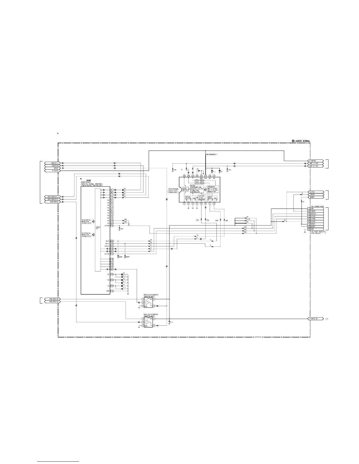
DIGITAL MAIN PWB ASS'Y(3/5)
FU-1ESA19805
DIGITAL MAIN PWB(2/5)
DIGITAL MAIN PWB(5/5)
A94N5SCD3_0430_3/5_0.0
The order of pins shown in this diagram is different from that of actual IC3301.
IC3301 is divided into
five
and shown as IC3301 (1/5) ~ IC3301 (5/5) in this Digital Main Schematic Diagram Section.
1 NOTE:
DIGITAL MAIN PWB(5/5)
DIGITAL MAIN PWB(5/5)
DIGITAL MAIN PWB(4/5)
OPEN
IC3301
C3055
C3056
C3057
C3058
R3041
R3803
IC3801
R3820 R3821
C3802
C3803 C3801
R3804
BC3801
R4101
R4102
R4105
R4104
R4106
R4103
R3155
R3809R3808
R3802
R3813
R3801
R3810
R3811
R3814
R3156
R3150
CN4101
R3042
R3043
R3828
R3829
R3830
R3831
R3832
C3829C3828
C3054
C3015
C3053
C3016
C3052
C3017
IC3303
IC3302
C3301
DIGITAL MAIN PWB CIRCUIT DIAGRAM (3/5)
This schematic is only for reference.
Avoid replacing individual parts.
Relpace the entire PWB ASS'Y only.
 Loading...