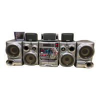
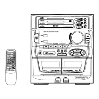
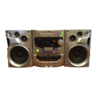
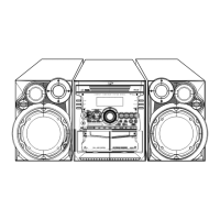
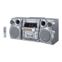
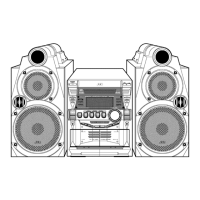
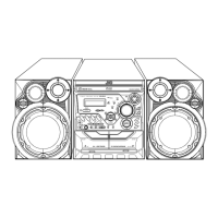
MX-DVB10
1-62
1. Pin layout
2. Block diagram
LV1100 (IC550) : Karaoke mic echo surround amp.
24 13~
112
~
3. Pin function
1 VSS
2
3
4
5
6
7
8
9
10
11
12
13
14
15
16
17
18
19
20
21
22
23
24
DATA
ENABLE
REV-OUT
REV-IN
VCC
IN-L
IN-R
IN-A
OUT-A
DC-OUT
LPF
VREF
OUT-R
OUT-L
AGND
DC-OUT
A/D
A/D
D/A
VDD
X2
X1
-
-
-
-
Pin No.
I/OSymbol
Function
Connect to GND
Power supply
Connect to GND
Power supply
CLOCK
I
O
I
I
I
I
I
O
O
O
O
O
I
I
I
I
I
I
O
I
Clock for communicated data
Amp. control data
Control signal enable
Analog signal input L
Analog signal input R
N.C.
N.C.
Reverse signal output
Reverse signal input
DC-output
External terminal for low pass filter
Reference voltage
Analog signal output R
Analog signal output L
External terminal for D/A
DC-output
External terminal for A/D
External terminal for A/D
External terminal for oscillator
External terminal for oscillator
OSC
REG
24
23
22
21
20
19
18
17
16
15
14
5KX2
L.P.F.
SRAM 12K
D/A CONV.
A/D CONV.
DC-CUT
DC-CUT
20PIN
19PIN
12PIN
18PIN
1
2
3
4
5
6
7
8
9
10
11
PIN
DEC
7KHZ L.P.F
EFECT VOL
REF
REF
REF
REF
REF
REF
REF
REF
REF
REF
REF
REF
REF
13
12