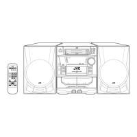
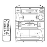
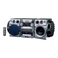
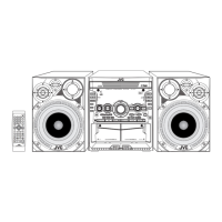
MX-J270V
1-39
1
2
3
4
5
6
7
8
9
10
11
12
13 15
16
17 24
25 39
40
41 48
49
50
51
52
53
54
55
56
57
58
59
60
61
62
63
64
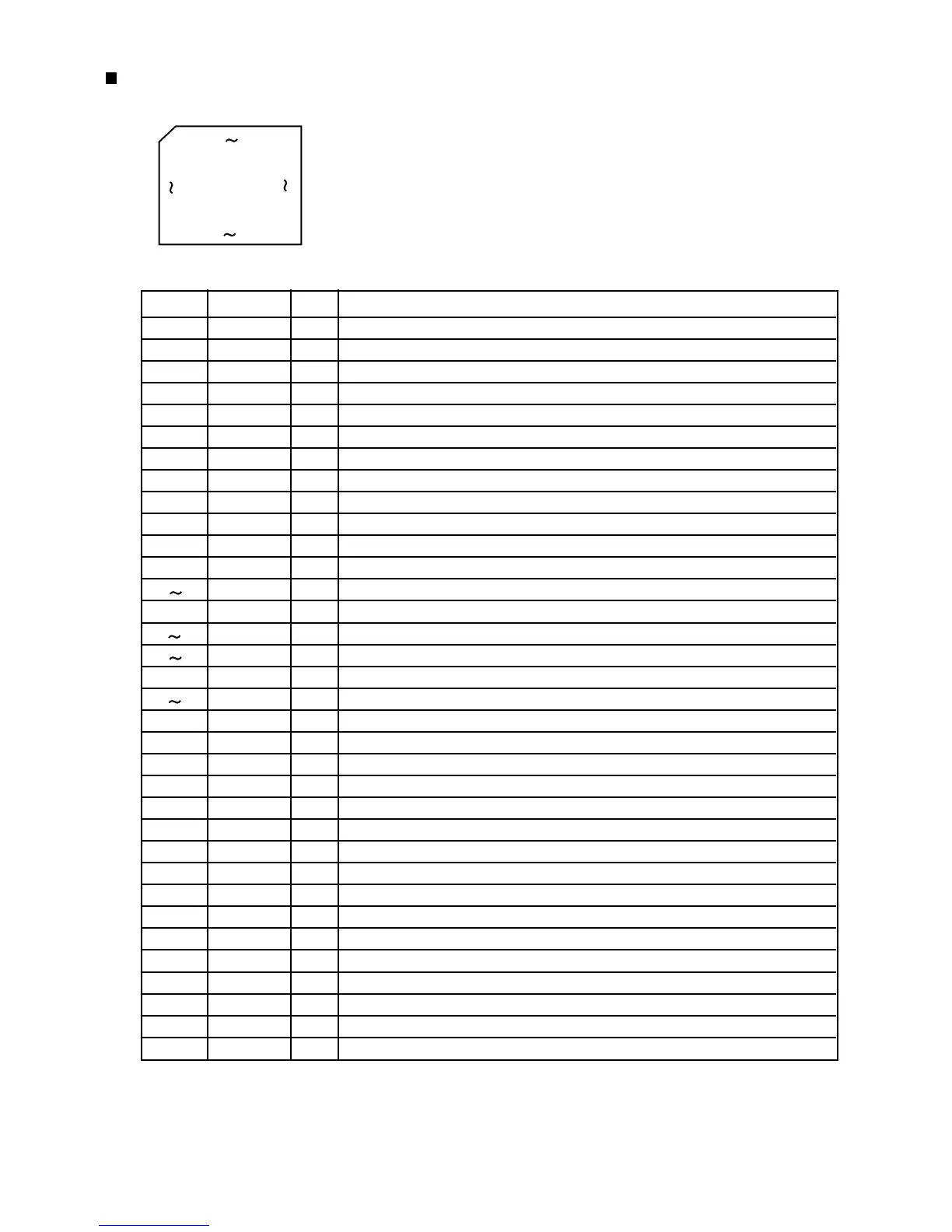
480RST
MREQ
ACTINT
GDET
GND
DTACK
GND
GND
DIR
N/PAL
RGB
W/R
HA02
DS
HD07
SA014
SCS
SD18
SR/W
PAL60
RESET
X1
X2
VSS
OSC2
OSC1
VDD
HREQ
SRCLK
M2HDT
M2MDT
HRDY
VCD/G
PALCDG
Reset signal output.
Input the transfer request data signal.
Interact 2 signal input.
CD-G detect terminal H:CD-G
Connected to GND.
Acknowledge signal input.
Connect to GND.
Connect to GND.
Input/Output control for IC114.
Not use.
Video out control signal (H:RGB L:composite)
Read/Write signal input/output.
Address signal output for MPEG LSI.
Data strobe signal output.
Data terminal for MPEG LSI.
SRAM address signal output.
SRAM chip select signal output.
SRAM data Input/Output terminal.
SRAM read/write signal input/output.
Not use.
Reset signal input.
Non connect
Non connect.
Connect to GND.
Non connect.
Clock input terminal.
Power supply.
Communication signal output.
Clock signal for data request.
Serial data output.
Serial data input.
Communication signal output.
Video swith switching signal output.
CD-G PAL/NTSC clock select terminal.
Pin No.
Symbol
I/O Function
O
I
I
I
-
I
-
-
I/O
-
O
I/O
O
O
I/O
O
O
I/O
I/O
-
I
-
-
-
-
I
-
O
O
O
I
O
O
O
MN171601AK8J2 (IC111) : HOST Micro Computer
1.Terminal Layout
2.Pin Function
1
16
48
33
17 32
64 49

 Loading...