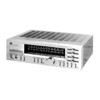
RX-508VBK
RX-509VTN
|
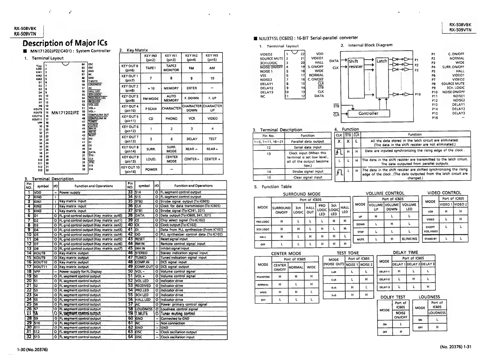
Description
of
Major
ICs
M
MN171202JPZ(IC401)
:
System
Controller
1.
Terminal
Layout
2.
Key
Matrix
KEY
INO
KEY
INI
KEY
IN2
KEY
IN3
(pin2)
(pin3)
(pina)
(pin5)
KEY
OUTO
TAPE2
KEY
OUT
1
7
{pin7)
KEY
OUT2
sg?
[
ve
[one
[ore
[=|
64
63
62
61
60
59
58
37
D4
56
i
i
KEY
OUT3
AUTO
ag
07
53
(pind)
MEMORY
:
o8
52
KEY
OUT4
cours
51
Ev
OuT4
|
scan
CHARACTER
CHARACTER
|
CHARACTER
crows
[15
MIN171202/PZ_
2
KEY
OUTS
“a
oat
°
my”
|__|
e¥ono
|
ver
|
vito
is
<
KEY
OUT6
;
$2
“a
{pin12)
$3
43
KEY
OUT?
.
42
:)
40
KEY
OUTS
SURR.
39
=-
3
38
wintay)
|
SUR
|
move
39
37
510
su
$12
$13
KEY
OUT9
CENTER
KEY
OUT
10
3.
Terminal
Description
te)
no.|
symbo!_|vo|
Function
and
Operations
JRo.|
symbot_|vo|
Function
and
Operations
|
T
fvop
|
~|Powersupply
SS
S140
[FL
segment
control
output
Pe
kino
84
15
0 |
FL
segment
control
output
[Skint
[1
[Key
matrix
input
35
fstB2____
©
[Strobe
signal
output
(To
1C605)
Seas
Pa
feina
[key
matrix
input]
36
eK
|
0
[Clock
for
data
transmission
(To
1C605)
_
Spans
[1
[key
matrix
input_______|
37
S81
[0
[strobe
signal(Toicsat,321)
_—~+|
T6_[oi
[©
|
Fi
grid
control
output
(Key
matrix
out0)_|
38
[DATA
[0
[Data
output
(Toiceos,341,
321)
_|
H--Jo2
0
JF
grid
controfoutput
(Key
matrix
outl)
|
39
[ce
[0
[Chip
select
signal
(Toicio2)
|
T'S
_[os
0
|FL. grid
control
output
(Key
matrix
out2)
|
40
[ck
[©
[Clock
output(Toici02)__————————id
L37Joa
[©
JFL
grid
control
output
(Key
matrix
outa)
|
41
[bi
|]
|
[Data
from
PLL
synthesizer
(From
iC102)_|
[10
[os
0
|r
grid
control
output
(Key
matrix
outa)
[42
[D0
|
O
[PLL
synthesizer
control
data
(ToIC102)_|
HIT [06
J
©
[FL
grid
control
output
(Key
matrix
outs)
|
43
[RESET
|
1
[Resetsignalinput
H12[o7
TO
]FL
grid
contro!
output
(Key
matrix
outé)_|
44
[RMIN
[1
[Remote
control
signal
input
HTS
[os
[0
]FL
grid
control
output
(Key
matrix
out?)
[45
INHIN
[1
inhibitsignalinput
Hid
ours
—[o
[key
matrix
output
_________|
46
BTEREO__|
1
[stereo
indication
signal
input____|
PTS[kouTs
[0
key
matrix
output
|
47
JTUNED
[1
|Tunedindication
signal
input]
[16
kOUTIO
[0
[Key
matrix
output
|
48
KOMPIN
[1
]OCS
signalinput
LTT
JeouTi1__|
0
[key
matrix
output________|
49
Come.ouT]
0
|cs
signal
output
———SSSCS—~S
[18
[ve>
|
—
[Power
supply
for
FL
Dsplay
|
SO
VOL-
[0
|Volume
control
signal
P13
fs0_____[O]Fi
segment
controloutput
|
51
Jvol+
[0
|Volume
control
signal___———*d
[2051
[0
[FL
segment
controfoutput________|
52
)VOLUED_[Oindicatordrve
SSCS
[21
[s2_____[O]FL
segment
controloutput_
|
53
[RECEIVED
[0
|indicatordrive———S—S
[22
[53____]O]FLsegmentcontroloutput______|
S@[PRO.LED
[O|indicatordrve
Sid
[23
[s4____
[0
|FL
segment
controloutput
|
55
SCHED
|
O|indicatordrve
SSCS
[2a
]s5__[O]FL
segment
controloutput____
|
56
HALLLED
|O|indicatordrve
_——_+
[2556
[0
[FL
segment
controloutput______[
57
JAC
O
|Power
primary
control
signal
|
TF
$8
{0
|
segmerteortoctot
[8
[MUTE
[Tuner
mueng
ert
Lit
ft
FC
Segmiert
contol
ONL
STMUTE
|
[Toner
mubng
contol
|
[2B
9
]O|FLsegmentcontroloutput__
|
60
|GND___|—|ConnectedtoGND_____——S~sS
[235100
|FL
segment
control
output
61
INC____|
-
JNonconnection
SY
[30j511__To
]Fi
segment
controloutput______|
62
J@nDJ-JenD_————SS~SCSCSS—
[31
B12
[O
[FL
segmentcontrotoutput
|
63
sc
|
-
|Clockoxcllationowtput_———S—~S
[32513
___[O]Fisegmentcontroloutput___]
64
Josc__|
~
[Clock
oscilationinput_____—
1-30
(No.20376)
RX-508VBK
RX-509VTN
HE
.NJU3715L
(IC605)
:
16-BIT
Serial-paraile!
converter
41.
Terminal
layout
2.
Internal
Block
Diagram
Me
MUTE
:
vicar
a
pony
U
3CHLOGIC
3
Hat.
PATA
[~?
|Shift
ne
ee
maces
NOISE
ON/OFF
|
4
$.
ON/OFF
aK
resister
P2
P4
—
SURR.
ON/OFF
NOISE
1
5
WIDE
P3
PS
HALL
VSS
6
NORMAL
P6
VIDEO
NOISE2
7
C.
ON/OFF
°7
VIDEO2
DELAY}
8
cLR
P8
SOURCE
MUTE
DELAY2
9
STB
Po
3CH.
LOGIC
DELAY3
0
cLK
P10
NOISE
ON/OFF
NC
1
DATA
PIG
P11
NOISE1
P12
NOISE2
1B
P13
DELAY?
es
P14
DELAY2
PI6
~
3.
Terminal
Description
4.
Function
Princ.
|___Fan]
4~5,7~11,16~21
Parallel
data
output
XTX
pk
All
the
data
stored
in
the
latch
circuit
are
eliminated.
(The
data
in
the
shift
resister
are
not
eliminated.)
Seria!
data
input
AL]
*
|
¥
|
Data
are
inputed
synchronizing
the
rising
edge
of
the
clock.
Pe
eB
Clock
input
(When
this
terminal
is
set
low
level,
-
The
data
in
the
shift
resister
are
transmitted
to
the
latch
circuit.
The
data
outputed
from
parallel
outputs.
all
of
the
output
become
low.)
The
data
in
the
shift
resister
are
shifted
synchronizing
the
rising
edge
of
the
clock
.(The
data
outputed
from
the
latch
circuit
are
[14
«|
__
Strobe
signal
input
__|
signal
input
fe
15
=
ih
Clear
signal
input
changed.)
5.
Function
Table
SURROUND
MODE
Port
of
IC605
HALL
OuT
freveef
»
fetes
VIDEO
CONTROL
Port
of
IC605
VIDEO
1
{VIDEO
2
Pe
te
|e
|
Powe
ff
|
EXCEPT
L
L
VCR,
VIDEO
VOLUME
CONTROL
Port
of
IC605
VOLUME
|
VOLUME}
VOLUME
uP
DOWN
LED
pete fete
|
[oom
[ef
e
|
|
Se
ce
TEST
TONE
DELAY
TIME
MODE
Port
of
1C605
Port
of
[C605
(No'se
oun]
Rose
[NOWE?|
Le
|
feel
fe
fe
foe
pw |e
|
PRO
|
3ch
ne
Logic
|Loaic|
WA
Led
|
LED
Port
of
IC605
(No.
20376)
1-31
 Loading...