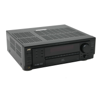
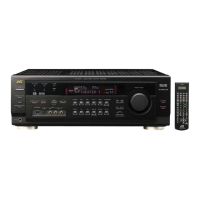
RX-807VTN
M@
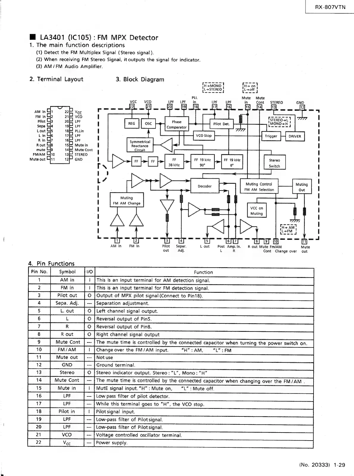
1A3401
(IC105)
:
FM
MPX
Detector
1.
The
main
function
descriptions
(1)
Detect
the
FM
Multiplex
Signal
(Stereo
signal).
(2)
When
receiving
FM
Stereo
Signal,
it
outputs
the
signal
for
indicator.
(3)
AM/FM
Audio
Amplifier.
2.
Terminal
Layout
3.
Block
Diagram
st
__.
[H>MONo
!
Fu
on}
pL>
STEREO
|
oot
y
PLL
Mute Mute
vcc
vco
LPF
LPF
in
LPF
LPF
in
Cont
STEREO
GND
pa---
2B
_
l
e
e
AM
in
Vec
FM
in
vco
A
(ten
b
1
Pilot
LPF
Phase
:
IMONO+H
!
ae
Be
tie
Ges
es
Lout
PLLin
R
in
LPF
Symmetrical
Reactance
Circuit
Rout
mute
FM/AM
Mute
out
4411
Le
FF
a
FF
19
kHz
fl
FF
19
kHz
Stereo
38
kHz
90°
0°
Switch
aa
i
|
I
]
I
i
I
I
I
a
|
ao
I
I
l
I
all
Mute
Cont
STEREO
GND
I
I
I
I
Mute
in
I
I
L
|
ee
|
|
Muting
#
i
I
FM
AM
Change
T
1
I
VCC
on
|
rh
Muting
|
I
4
Pe.
ian?
orm
L
=—
=
=
aes
— = —
—
2
|
4
|
5
|
6
|
"Ts!
GT
fq
AM
in
FM
in
Pilot
Separ.
L
out
Post
Amp.in.
R
out
Mute
Fm/AM
Mute
R
Cont
Change
over
out
Pin
Functions
[7
[This
i
an
input
terminal
for
AM
detection
signal,
————SSSCSC~SCSCS
[1
[This
is
an
input
terminal
for
FM
detection
signal
SSCS
[0
[output
of
MPX
pilot
signal
(Connect
to
Pin'g).
SSCS
canal
[=
JSeparation
adustment,
SS
SOSCSCSCSCSCSSCSC“‘“S*S*S~S~*Y
Ps
[tout
[6
[lett
channel
signal
outst
————SSSCCSC~CSCSCSSCSCCSCSC
[o
[Reversal
ouput
of
ins.
SSCSCSCSCSCSCSC“SCS*C“‘*S*S*~S*S
To
[Reversal
output
of
Ping.
SSSSCSCSCSCSCSCSC“‘“‘S*S*S*S*~“~S~S~S
[8
[Rout
[0
[right
channel
signal
output
SSSCSCSCSCSCSCSCSCSSSSSC*?r
[9
|
“mute
Cont
|-—
[The
mute
time
is
controlled
by
the
connected
capactor
when
turning
the
power
switch
on.
|
|
10
[|
FMsam
|
|
Change
over
the
FM/AM
input.
“H"
>
AM,
“LYS
FM
Pit
[ute
out
[—[notwe
OCS
pz
[
en
|=
Joroundtermings—SSSOSCSCSCSCSCSCSCCCCSS
|
13
|
Stereo
|
0
|
Stereo
indicator
output.
Stereo:
"L",
Mono:
“H”
|
14
|
Mute
Cont
|---|
The
mute
time
is
controlled
by
the
connected
capacitor
when
changing
over
the
FM/AM
.
|
15
|
Mutein
|
1
|
MutE
signal
input.“H"
:
Mute
on,
“L”
:
Mute
off.
[=
|lewraesfter
of
pt
dete,
|
|
While
this
terminal
goes
to
“H”,
the
VCO
stop.
ee
|
mean
S|
iscsaralngne
La
|e
is
lone
tne
ere
=
ieee
ter
of
Pickignal
J
|
21
|
veo
||
Voltage
controlled
oscillator
terminal.
cc
|
---
|
(No.
20333)
1-29
 Loading...