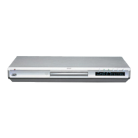
XV-N50BK,XV-N55SL
(No.A0041)1-27
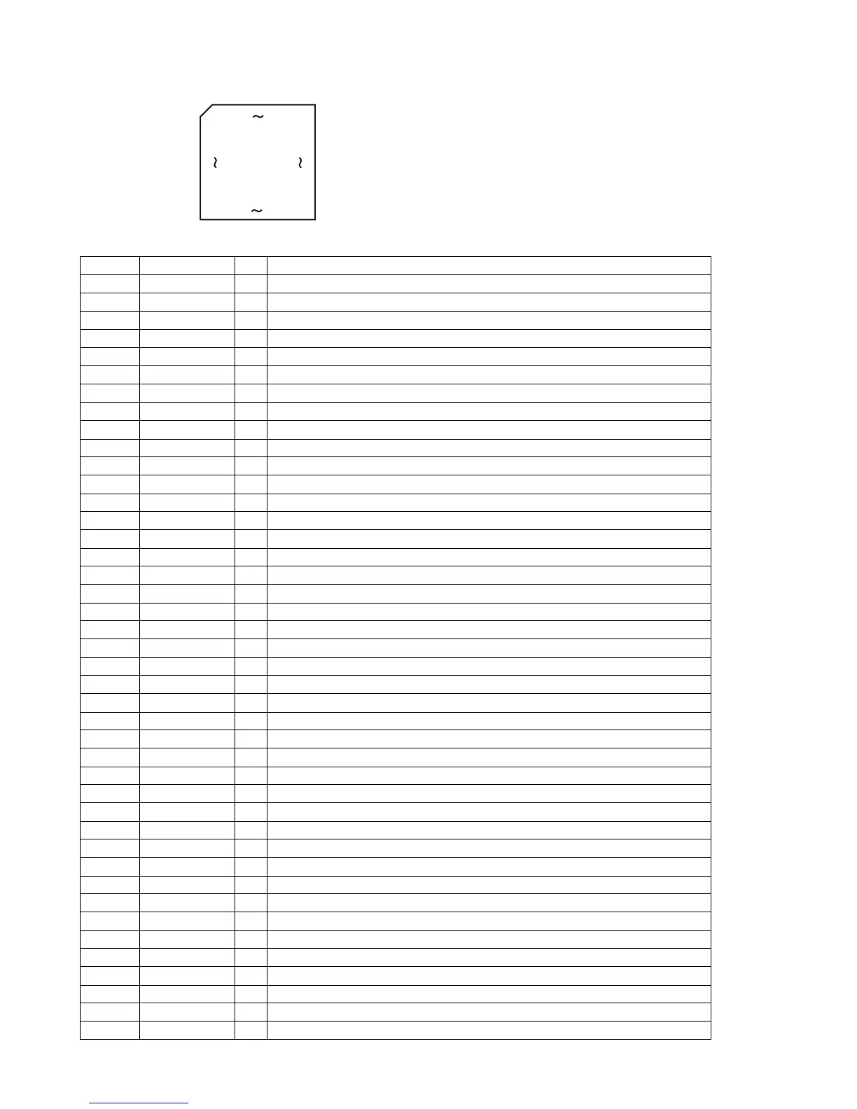
4.3 AN8708FHK(IC101):Frontend processor
•Pin layout
• Pin function
1
12
36
25
48 37
13 24
Pin No. Symbol I/O Description
1 GND1 - Connect to ground
2 LPC1 I Laser input terminal (DVD)
3 LPC01 O Laser drive output terminal (DVD)
4 LPC2 I Laser input terminal (CD)
5 LPC02 O Laser drive output terminal (CD)
6 FBAL I Focus balance control terminal
7 TBAL I Tracking balance control terminal
8 POFLT O Track detection filter terminal
9 SEN I SEN (Serial data input terminal)
10 SCK I SCK (Serial data input terminal)
11 STDI I/O STDI (Serial data input/output terminal)
12 VRE18 - RF Standard voltage filter
13 TE O Tracking error signal output terminal
14 VSS - Connect to ground
15 OFTR O OFTR output
16 BDO O BDO output
17 VDD - Power supply terminal 3 (3.3V)
18 RSCL - Source terminal of standard current
19 GND2 - Connect to ground
20 FE O Focus error signal output terminal
21 FS O Focus addition signal output terminal
22 VHALF O VHALF Voltage output terminal
23 MIRSL O MIRROR Slow envelope detection terminal
24 BDOSL O BDO Slow envelope detection terminal
25 VCC2 - Power supply terminal 2 (3.3V)
26 FLTOP O Filter amplifier positive output terminal
27 FLTON O Filter amplifier negative output terminal
28 SAG O SAG Cancel detention terminal
29 DCAGC O FLT-DC Cut filter terminal
30 AGCG O AGC Amp.gain control terminal
31 TESTSG I TEST signal input terminal
32 RFINP I RF signal positive input terminal
33 RFINN I RF signal negative input terminal
34 DCRF O Filter terminal for RF all addition AMP.DC cut
35 PEAK O Peak envelope detection filter terminal
36 RFENV O RF Envelope output terminal
37 VCC1 - Power supply terminal 2 (5V)
38,39 VIN5,6 I Internal four division (CD) RF input terminal 1,2
40,41 VIN7,8 I External two division (DVD) RF input terminal 1,2
42 VREF - VREF Voltage output terminal
43~46 VIN1~4 I Internal four division (DVD) RF input terminal 1~4
47,48 VIN9,10 I Three beam sub (CD) input terminal 1,2
 Loading...