XV-N50BK,XV-N55SL
1-28 (No.A0041)
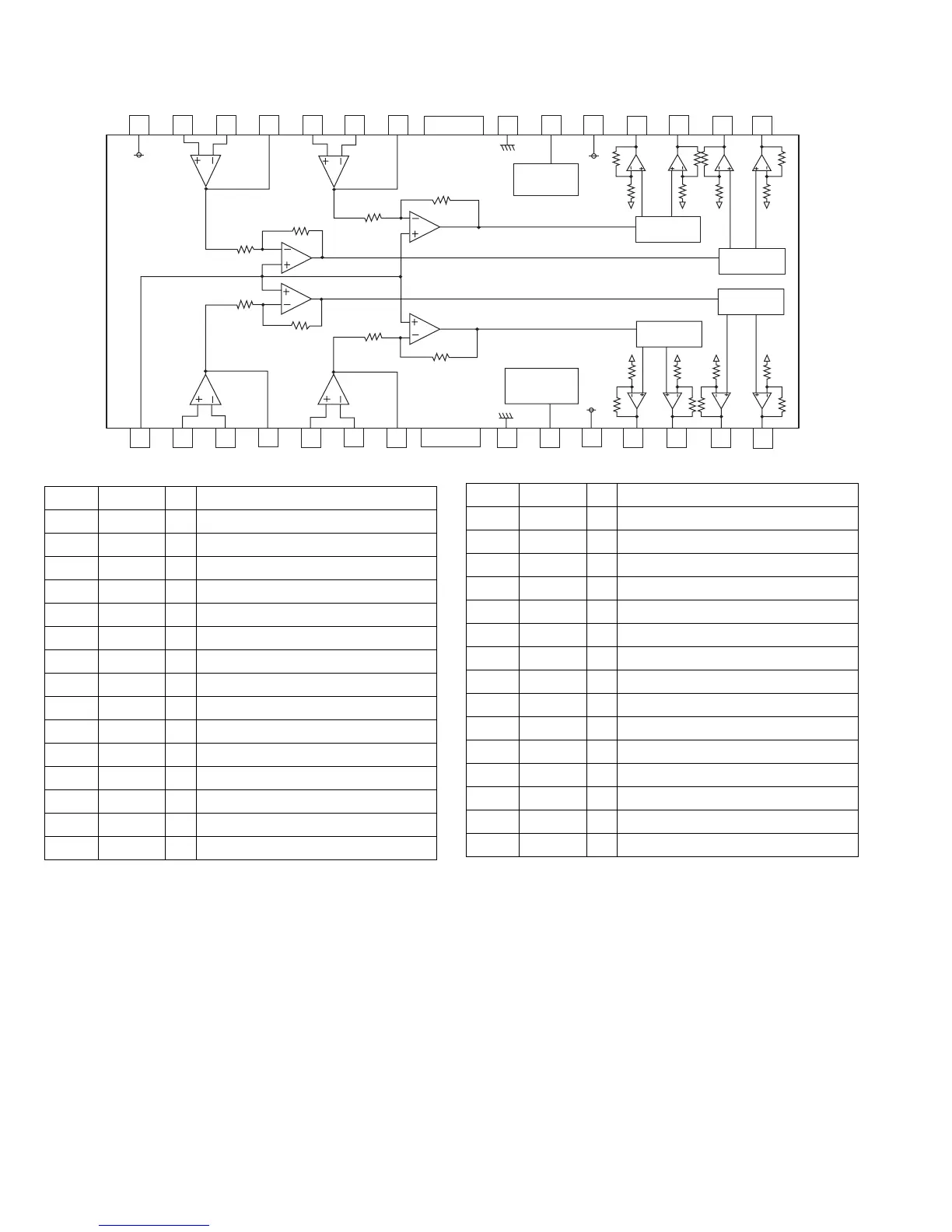
4.4 BA5983FM-X (IC201) : 4-channel driver
• Block diagram
• Pin function
28
27
26
Vcc
25
24
23 22 30
10k
20k
21
20
19
18
17 16
15
STAND BY
CH4
Vcc
10k
10k
Vcc
Level Shift
Level Shift
Level Shift
Level Shift
STAND BY
CH1/2/3
10k
10k
10k
10k
10k
20k
1
2
3
4
5
6
729 891011121314
10k
10k
10k
10k
10k
10k
10k
10k
10k
10k
10k
10k
10k
10k
Pin No. Symbol I/O Description
1 BIAS IN I Input for Bias-amplifier
2 OPIN1(+) I Non inverting input for CH1 OP-AMP
3 OPIN1(-) I Inverting input for CH1 OP-AMP
4 OPOUT1 O Output for CH1 OP-AMP
5 OPIN2(+) I Non inverting input for CH2 OP-AMP
6 OPIN2(-) I Inverting input for CH2 OP-AMP
7 OPOUT2 O Output for CH2 OP-AMP
8 GND - Substrate ground
9 STBY1 I Input for CH1/2/3 stand by control
10 PowVcc1 - Vcc for CH1/2 power block
11 VO2(-) O Inverted output of CH2
12 VO2(+) O Non inverted output of CH2
13 VO1(-) O Inverted output of CH1
14 VO1(+) O Non inverted output of CH1
15 VO4(+) O Non inverted output of CH4
16 VO4(-) O Inverted output of CH4
17 VO3(+) O Non inverted output of CH3
18 VO3(-) O Inverted output of CH3
19 PowVcc2 - Vcc for CH3/4 power block
20 STBY2 I Input for Ch4 stand by control
21 GND - Substrate ground
22 OPOUT3 O Output for CH3 OP-AMP
23 OPIN3(-) I Inverting input for CH3 OP-AMP
24 OPIN3(+) I Non inverting input for CH3 OP-AMP
25 OPOUT4 O Output for CH4 OP-AMP
26 OPIN4(-) I Inverting input for CH4 OP-AMP
27 OPIN4(+) I Non inverting input for CH4 OP-AMP
28 PreVcc - Vcc for pre block
29 - Connect to ground
30 - Connect to ground
Pin No. Symbol I/O Description
 Loading...