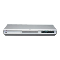
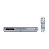
XV-N50BK,XV-N55SL
(No.A0041)1-37
4.9 PT6315(IC801):FL Display driverBlock diagram
• Block diagram
• Pin function
Pin No. Symbol I/O Description
1 to 4 LED1 to LED4 O LED Output Pin
5 OSC I Oscillator Input Pin
A resistor is connected to this pin to determine the oscillation frequency
6 DOUT O Data Output Pin(N-Channel, Open-Drain)
This pin outputs serial data at the falling edge of the shift clock(starting from the lower
bit)
7 DIN (Schmitt Trigger) I Data Output Pin
This pin inputs serial data at the rising edge of the shift clock(starting from the lower bit)
8 CLK (Schmitt Trigger) I Clock Input Pin
This pin reads serial data at the rising edge and outputs data at the falling edge.
9 STB (Schmitt Trigger) I Serial Interface Strobe Pin
The data input after the STB has fallen is processed as a command.
When this pin is "HIGH",CLK is ignored.
10,11 K1 to K2 I Key Data Input Pins
The data inputted to these pins are latched at the end of the display cycle.
12,44 VSS - Logic Ground Pin
13,43 VDD - Logic Power Supply
14 to 29 SG1/KS1 to SG16/KS16 O High-Voltage Segment Output Pins
Also acts as the Key Source
30 VEE - Pull-Down Level
31 to 38 SG17/GR12 to SG24/GR5 O High Voltage Segment/Grid Output Pins
39 to 42 GR4 to GR1 O High Voltage Grid Output Pins
DIN
DOUT
CLK
STB
OSC
R
LED1
LED2
LED3
LED4
K1
K2
VDD
GND
VEE
Segment
Driver/
Grid
Driver/
Key Scan
Output
Grid
Driver/
Dimming Circuit
Key Matrix
Memory
Timing Generator
Display Memory
(24bits x 12 Words)
Control
Serial
Data
Interface
OSC
LED
Driver
SG1/KS1
SG16/KS16
~
SG17/GR12
SG24/GR5
~
GR1
GR4
~
 Loading...