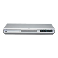
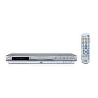
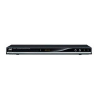
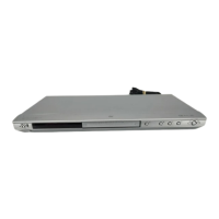
XV-N50BK,XV-N55SL
1-38 (No.A0041)
4.10 UPD789074MC-026(IC701):System controller
• Pin layout
• Pin function
NTB
S/COMP
VPP
RESET
X2
X1
VSS
VDD
TCLOSE
TOPEN
AVCI
REMO
SWCLOSE
SWOPEN
RXD
PROG
INT
GAINCONT
E/OTHER
LMUTE
AVCO
P.ON/STANDB
CPURST
MUTE
FLDIN
FLDOUT
FLCLK
FLSTB
INTP
TXD
1
2
3
4
5
6
7
8
9
10
11
12
13
14
15
30
29
28
27
26
25
24
23
22
21
20
19
18
17
16
Pin No. Symbol I/O Description
1 NTB I COMP/RGB-Y/C or PAL-NTSC Change signal input terminal
2 S/COMP I S(L)/COMPORNENT(H) output switching signal input
3 VPP - The power supply for on board to writing
4 RESET I Reset input (L:reset)
5 X2 - Clock (5MHz)
6 X1 - Clock (5MHz)
7 VSS - Connect to ground
8 VDD - Power supply terminal +3.3V
9 TCLOSE O PWM signal output for tray close
10 TOPEN O PWM signal output for tray open
11 AVCI I AV Compulink control data input
12 REMO I Remote control signal input
13 SWCLOSE I Tray switch signal input 1 L:Full open L:Movement H:Full close
14 SWOPEN I Tray switch signal input 2 L:Full open H:Movement H:Full close
15 RXD I Decoder serial communication data input
16 TXD O Decoder serial communication data output
17 INTP O Decoder serial communication interruption signal output
18 FLSTB O FL Driver strobe output
19 FLCLK O FL Driver clock output
20 FLDOUT I Data input from FL Driver
21 FLDIN O Data output to FL Driver
22 MUTE O Audio muting output H:muting
23 CPURST O LSI Reset output L:reset
24 P.ON/STANDB O Power ON output
25 AVCO O AV Compulink control data output
26 LMUTE O Motor driver muting output H:mute
27 E/OTHER I Destination detection terminal Europe or Other
28 GAINCONT O Gain control signal
29 INT I INT/PROG Change signal input terminal H:Interlace
30 PROG I INT/PROG Change signal input terminal H:Progressive
 Loading...