SECTION2
Operation
+
~:
r-------.
1
-JVvVv\r-....,
1
---1~---o
Output
HI
R'
)'
~
- >
.....
Av
?
Cour
I
V
Source
I
1...._
_______
....,...
__
-o
Output
LO
R'
= Current range resistor
Av
=Loop
gain
(106)
R'
L'
=
21tBW'
BW
=40kHz
for 1.1V, 1.5V, 11V, 15V and
11
OV
ranges
= 4 kHz for
11
OOV
range
Cour
=Fixed
capacitor (depends on selected current range)
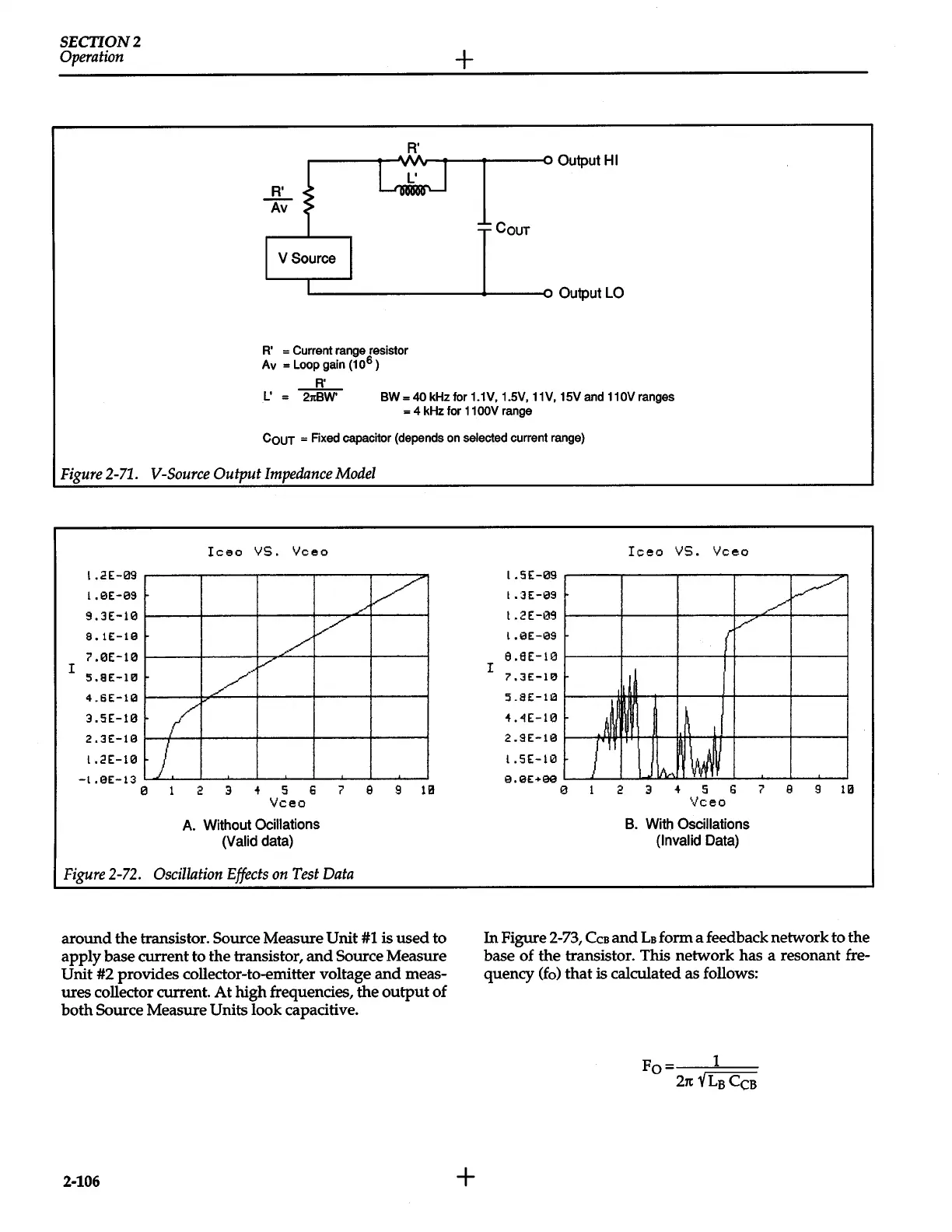
Figure
2-71.
V-Source
Output
Impedance
Model
!ceo
VS.
Vceo
!ceo
VS.
Vceo
I
.2E-09
I
.aE-09
9.3E-10
8.1E-18
7.0E-10
I
5.8E-111J
4.sr-ua
/
/
_../
/
/.~
/
l
.5E-09
l
.JE-09
l
.2E-09
1
.ar-es
e.eE-10
I
7.3E-10
s.ar-ua
r/
3.5E-10
2.3E-19
I.C!E-10
-1
.aE-13
(
)
i."'E-10
2.SE-18
l.5E-10
A
J
~
v~
~
~/
1:3
2
3 4
5
6 7 9 9
18
e.aE+ae
0
2 3 4
5
6 7
9
9
Hl
Vceo
A.
Without
Ocillations
(Valid
data)
Figure
2-72.
Oscillation
Effects
on
Test
Data
around
the
transistor. Source Measure
Unit
#1
is
used
to
apply
base current to
the
transistor,
and
Source Measure
Unit
#2 provides collector-to-emitter voltage
and
meas-
ures collector current.
At
high frequencies,
the
output
of
both
Source Measure Units
look capacitive.
2-106
+
Vceo
B.
With
Oscillations
(Invalid
Data)
In
Figure 2-73,
Ccs
and
Ls
form a feedback network to the
base
of
the transistor. This
network
has a resonant
fre-
quency
(fo)
that
is calculated as follows:
1
Fo
21t
VLBCcB
 Loading...