7
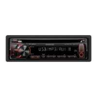
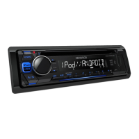
KDC-2031SA/2031SAY
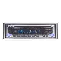
KDC-2031SG/2031SGY
● CD MECHANISM µ-COM : IC2 on X32- (CD PLAYER UNIT)
Pin No.
Active
Pin Name I/O Application Processing Operation
(H/L)
1 TVD O Traverse drive output (PWM output).
2 SPL O Spindle motor drive output (PWM output).
3NC-No connection.
4 PWM O Multipurpose PWM output.
5 TBAL O Tracking balance adjustment output (PWM output).
6 FBAL O Focusing balance adjustment output (PWM output).
7 NRFDET I RF detection signal input. L : Detection
8 OFT I Off-tracking signal input. H : Detection
9 BDO I Drop-out signal input. H : Detection
10 LDON O Laser-on signal output. H : Focus ON
11 DSLB O DSL balance output.
12 DVDD1 - Power supply for digital circuit.
13 DVSS1 - GND for digital circuit.
14 AVSS2 - GND for analog circuit. For DSL, PLL and A/D converter
15 DSLF I/O Loup filter for DSL and bias output for ARF.
16 ARF I RF signal input.
17 RFSW I DSL circuit time constant switch.
18 PLLF I/O Loup filter for PLL.
19 PLLF2 I/O Loup filter character switch for PLL.
20 IREF I Reference current input.
21 RFENV I RF envelope signal input.
22 TRCRS I Tracking cross signal input.
23 TE I Tracking error signal input.
24 FE I Focusing error signal input.
25 AVDD2 - Power supply for analog circuit. For DSL, PLL and A/D converter
26 AVSS1 - GND for analog circuit. For Lch/Rch audio output
27 OUTR O Rch audio output.
28 AVDD1 - Power supply for analog circuit. For Lch/Rch audio output
29 OUTL O Lch audio output.
30 DVSS3 - GND for digital circuit.
31 CSEL -
32 NC - No connection.
33 ASEL -
34 MSEL0 -
35 MSEL1 -
36~39 NC - No connection.
40 VREFP - Reference power supply input for A/D converter.
41 HOT -
MICROCOMPUTER’S TERMINAL DESCRIPTION
w
w
w
.
x
i
a
o
y
u
1
6
3
.
c
o
m
Q
Q
3
7
6
3
1
5
1
5
0
9
9
2
8
9
4
2
9
8
T
E
L
1
3
9
4
2
2
9
6
5
1
3
9
9
2
8
9
4
2
9
8
0
5
1
5
1
3
6
7
3
Q
Q
TEL 13942296513 QQ 376315150 892498299
TEL 13942296513 QQ 376315150 892498299
 Loading...