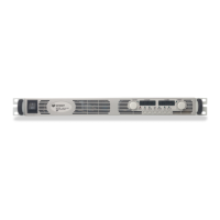
8
Instrument Memory
This section contains information on the types of memory available in your instrument. It explains
the size of memory, how it is used, its location, volatility, and the sanitization procedure.
Table 1: Summary of instrument memory for the DC Power Supply.
Memory Type
and Size
Is Memory user
accessible as a mass
storage device?
Writable During Normal
Operation?
Data Retained When
Powered Off?
Purpose/Contents
Data Input
Method
Location in
Instrument and
Remarks
Sanitization
Procedure
(NAND Flash)
42 MB
operating system
and instrument
firwmare
Install /
Firmware
Upgrade
user accessible,
and contains no
application-
specific
User Flash
(NAND Flash)
(Keysight Flash)
Yes Yes Yes saved instrument
states and
calibration
User-saved
data
CPU board (same
chip as firmware
memory, but
See Table 2
(Keysight
Flash2)
1 MB
Service Only
chip as firmware
memory, but
managed separately
user accessible,
and contains no
application-
specific
6 Mb
components that
load the operating
firmware from the
NAND flash memory
Install
chip as firmware
memory, but
managed separately
user accessible,
and contains no
application-
specific
FPGA
No Yes No GPIB control data
Factory
CPU board
Power cycle
Flash
No No Yes FPGA configuration
Factory
CPU board
No method, not
PROM
M25P40 FLASH
Memory
No Yes Yes FPGA program code.
No user stored data.
Factory
Service Only
CPU board No method, not
user accessible
Main processor
(ROM)
32 kB
No No Yes
Main processor
execution code
Manufacturer
programmed
user accessible,
and contains no
application-
specific