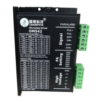
DM542 Fully Digital Stepper Drive Manual DM542 Fully Digital Stepper Drive Manual
5 6
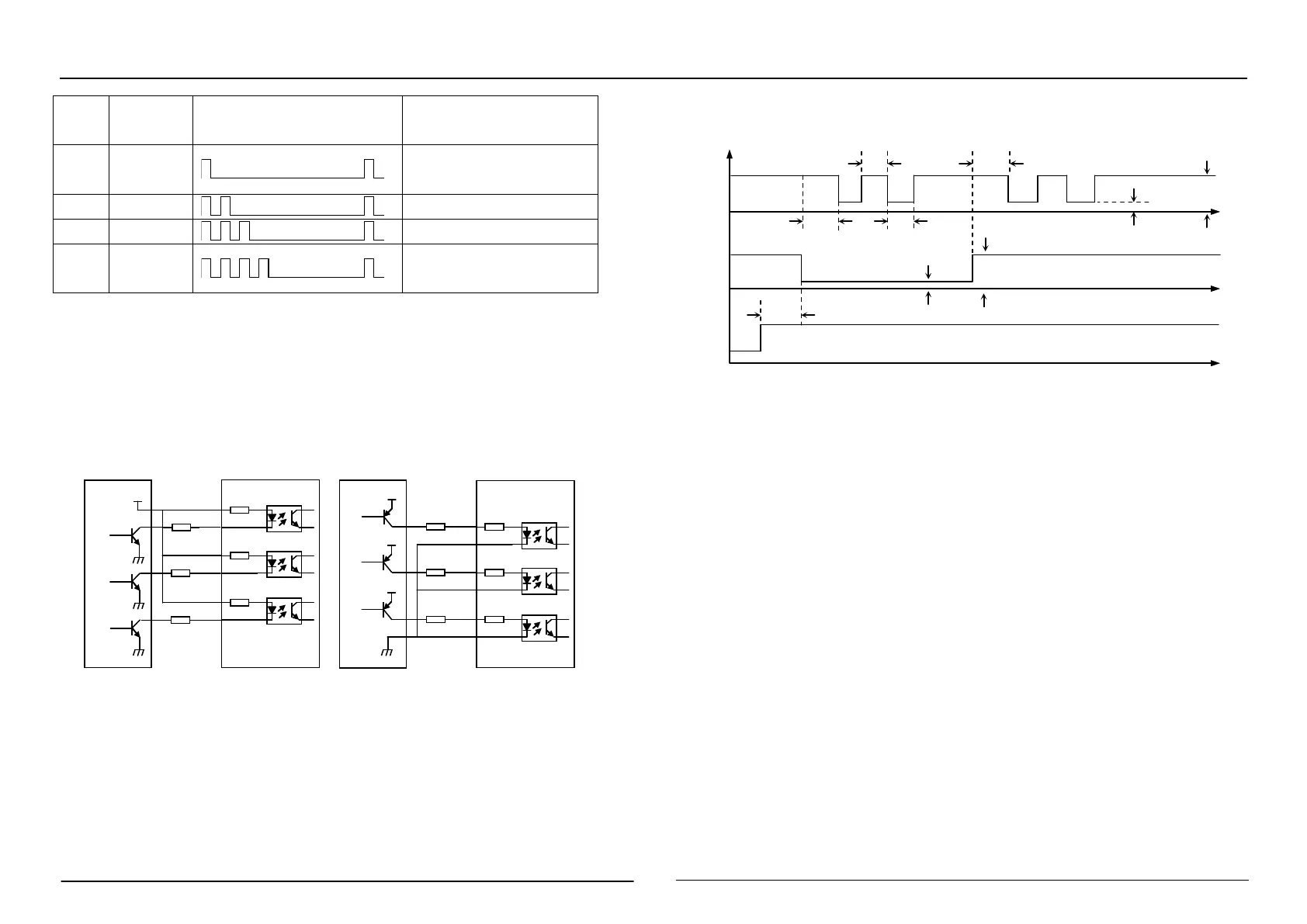
2. Control Signal Connector Interface
The DM542 driver uses a differential interface circuit for differential signaling, single-ended
common-cathode and single-ended common anode interfaces, and a built-in high-speed optocoupler
that accepts signals from long-line drivers, open collectors, and PNP output circuits. In the harsh
environment, we recommend long-line driver circuit, anti-interference ability. Now take the open
collector and PNP output as an example. The interface circuit is as follows:
Note: When the VCC value is 4.5~28Vdc, R is shorted or not connected;
3. Sequence Chart of Control Signals
In order to avoid some fault operations and deviations, PUL, DIR and ENA should abide by
some rules, shown as following diagram:
Remark:
a) t1: ENA must be ahead of DIR by at least 5
- are NC (not
connected). See “Connector P1 Configurations” for more information.
2)b)t2: DIR must be ahead of PUL effective edge by 2s to ensure correct direction;
3)c t3: Pulse width not less than 2s;
4)d)t4: Low level width not less than 2s.
4.
Control signal mode setting
Pulse Trigger Edge and Single and Double Pulse Selection: The pulse rising edge or falling edge
trigger is enabled by the PC software ProTuner software or STU debugger. It is also possible to set
the single pulse mode or the double pulse mode. In dual pulse mode, the signal from the direction
control must be held high or left floating.
5.
1)In order to prevent the driver from being disturbed, it is recommended to use the shielded cable
for the control signal, and the shield layer is shorted to the ground wire. Unless otherwise
specified, the shielded cable of the control signal cable is grounded at one end: the upper end of
the shielded cable is grounded at one end, and the shielded cable is driven. One end is suspended.
Only the grounding at the same point is allowed in the same machine. If it is not a real grounding
wire, the interference may be serious. At this time, the shielding layer is not connected.
NO. number of
flashes
Red LED flashing waveform Fault description
1 1
Overcurrent or phase-to-phase
short circuit fault
2 2
Overvoltage fault
3 3
No definition
4 4
Open motor or poor contact
failure
Connections to open-collector
signal (common-anode) (common-cathode)
2
us
2us
High level>3.5V
igh level>3.5V
ow level<0.5V
ow lever<0.5V
Figure 4 control signal timing diagram