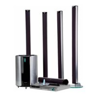
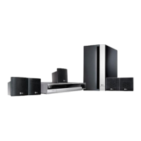
Do you have a question about the LG LH-W551TB and is the answer not in the manual?
Guidelines for handling the pick-up and general servicing notes.
Measures to protect against static discharge damage to sensitive components.
Flowchart for diagnosing audio system issues.
Troubleshooting flowchart for the front panel circuit (1/2).
Troubleshooting flowchart for the front panel circuit (2/2).
Diagram illustrating internal connections between PCBs and components.
High-level overview of system components and their interconnections.
Detailed circuit diagrams for the power supply unit.
Circuit diagram for the microcontroller unit.
Circuit diagram for the front panel assembly.
Circuit diagram for the Digital Signal Processor and Amplifier sections.
Circuit diagram for input/output interfaces.
Circuit diagram for the main microphone input section.
Component layout for the main/DVD PCB, top side.
Component layout for the main/DVD PCB, bottom side.
Component layout for the front microphone PCB.
Component layouts for the SMPS and Microphone PCBs.
Component layout for the amplifier PCB.
Flowchart illustrating the system's startup and basic operation sequence.
Flowchart for testing and debugging the system's functionality.
Troubleshooting flowchart for the audio microcontroller circuit.
Waveforms for system clock, reset, and flash read/write signals.
Waveform for the SDRAM clock signal.
Waveforms illustrating tray open and close operations.
Waveforms related to sled motor control in no disc condition.
Waveforms for lens control signals in no disc condition.
Waveforms showing disc type detection for DVD and CD.
Waveforms illustrating focus control signals for DVD and CD.
Waveforms for spindle motor control in no disc condition.
Waveforms of the RF signal for CD and DVD playback.
Waveforms of video output signals from the ES6698FD chip.
Waveforms of audio output signals from the PWM IC.
Waveforms related to DVD and amplifier signal checks.
Exploded view of the unit's cabinet and main frame components.
Exploded view of the disc deck mechanism.
Diagram of included accessories and packing materials.
Exploded view and parts for the center speaker.
Exploded view and parts for the front/rear speakers.
Exploded view and parts for the subwoofer speaker.
Exploded view of the wireless transmitter (ACC55T).
Exploded view of the wireless receiver (ACC55R).
Block diagram of the wireless transmitter module's electrical functions.
Block diagram of the transmitter's sub-circuit components.
First part of the transmitter module's circuit schematic.
Second part of the transmitter module's circuit schematic.
Third part of the transmitter module's circuit schematic.
Circuit schematic for the transmitter's sub-circuit.
Component layout for the transmitter module's upper side.
Component layout for the transmitter module's lower side.
Printed circuit diagram for the transmitter.
Block diagram of the wireless receiver module's electrical functions.
First part of the receiver module's circuit schematic.
Second part of the receiver module's circuit schematic.
Third part of the receiver module's circuit schematic.
First part of the receiver amplifier schematic.
Second part of the receiver amplifier schematic.
Third part of the receiver amplifier schematic.
Circuit schematic combining receiver module and amplifier.
Circuit schematic for the receiver's SMPS (power supply).
Component layout for the receiver module's upper side.
Component layout for the receiver module's lower side.
Component layout for the amplifier's upper side.
Component layout for the receiver SMPS (component side).