7
Effects board
EFX SEND 2
EFX SEND 2
EFX
SELECT
STEREO EFX
RETURN 2
RIGHT
STEREO EFX
RETURN 2 LEFT
EFX TO MAIN MIX
EFX TO AUX 1
EFX TO AUX 2
TO LEFT MAIN
TO RIGHT MAIN
EFX 2
EFX 1
AUX 2
AUX 1
DAMPING/DEPTH
TIME/RATE
EFX WIDE
EFX BYPASS
EFX BYPASS
EFX
FOOT
SWITCH
+5
VDC
EMAC
DSP
EFX LEVEL SET
L
R
BLOCK DIAGRAM
CLIP
WIDE BYPASS
100
100
REVERBS
DELAYS
CHORUS/FLANGE/PHASER
DAMPING
DEPTH
TIME
RATE
NORMAL NORMAL
EFX
SM. ROOM
MD. PLATE
LG. PLATE
LG. HALL
GATED
REVERSE
CATHEDRAL
MD. HALL
SPRING
PHASER
DELAY 4
CHORUS
DELAY 3
DELAY 1
FLANGE
DELAY 2
U
+15
OO
U
+15
OO
U
+15
OO
U
+15
OO
EFX 2 (INT) RETURN MASTERS
EFX
2
SEND
TO MAIN MIX
EFFECTS TO MONITOR
AUX
1
AUX
2
CUSTOM 32-BIT PRECISION
DIGITAL STEREO EFFECTS PROCESSOR
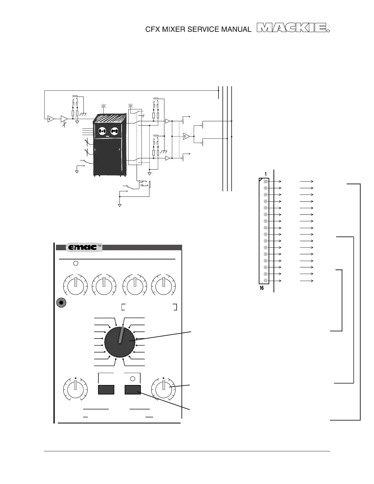
Adjustment of the rotary encoder S1 will vary the
level of BIT 0 through to BIT 3. This will select which
DSP algorithm is in effect on the EFX board’s DSP
IC U2.
The adjustment of these two pots directly affects
the CODEC IC U3. The levels are named POT 1 and
POT 2 at connector J1.
The state of the WIDE switch and the BYPASS
switch directly affect the DSP IC . The WIDE status
is named BANK. The BYPASS status is named FLAG.
J1-1
J1-2
J1
J1-3
J1-4
J1-5
J1-6
J1-7
J1-8
J1-9
J1-10
J1-11
J1-12
J1-13
J1-14
J1-15
J1-16
FLAG IN
BANK
+5V
DGND
MONO IN
AGND
RIGHT OUT
LEFT OUT
POT1
POT2
CLIP_LED
N/C
BIT 0
BIT 1
BIT 2
BIT 3
This shows the signals present on
the EFX board connector J1.
EFX CONTROLS


 To Next Page