21
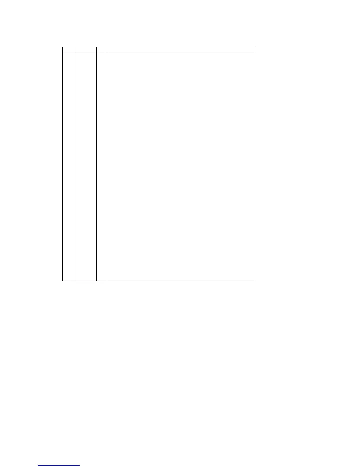
Figure 7-16
Pin configuration and description
No. Pin Name I/O Function
1
DVSS - Digital Ground Pin
2
DVDD - Digital Power Supply Pin, 3.3V or 5.0V
3
MCLK I Master Clock Input Pin
4
PDN I Power-Down Mode Pin
When at "L", the AK4393 is in power-down mode and is held in reset.
The AK4393 should always be reset upon power-up.
5
BICK I Audio Serial Data Clock Pin
The clock of 64fs or more than is recommended to be input on this pin.
6
SDATA I Audio Serial Data Input Pin
2’s complement MSB-first data is input on this pin.
7
LRCK I L/R Clock Pin
8
SMUTE I Soft Mute Pin in parallel mode
When this pin goes "H", soft mute cycle is initiated.
CSN I Chip Select Pin in serial mode
9
DFS I Double Speed Sampling Mode Pin (Internal pull-down pin)
"L": Normal Speed , "H": Double Speed
10 DEM0 I De-emphasis Enable Pin in parallel mode
CCLK I Control Data Clock Pin in serial mode
11 DEM1 I De-emphasis Enable Pin in parallel mode
CDTI I Control Data Input Pin in serial mode
12 DIF0 I Digital Input Format Pin
13 DIF1 I Digital Input Format Pin
14 DIF2 I Digital Input Format Pin
15 BVSS - Substrate Ground Pin, 0V
16 VREFL I Low Level Voltage Reference Input Pin
17 VREFH I High Level Voltage Reference Input Pin
18 AVDD - Analog Power Supply Pin, 5.0V
19 AVSS - Analog Ground Pin, 0V
20 AOUTR- O Rch Negative analog output Pin
21 AOUTR+ O Rch Positive analog output Pin
22 AOUTL- O Lch Negative analog output Pin
23 AOUTL+ O Lch Positive analog output Pin
24 VCOM O Common Voltage Output Pin, 2.6V
25 P/S I Parallel/Serial Select Pin (Internal pull-up pin)
"L": Serial control mode, "H": Parallel control mode
26 CKS0 I Master Clock Select Pin
27 CKS1 I Master Clock Select Pin
28 CKS2 I Master Clock Select Pin
Note: All input pins except internal pull-up/down pins should not be left floating.
 Loading...