15
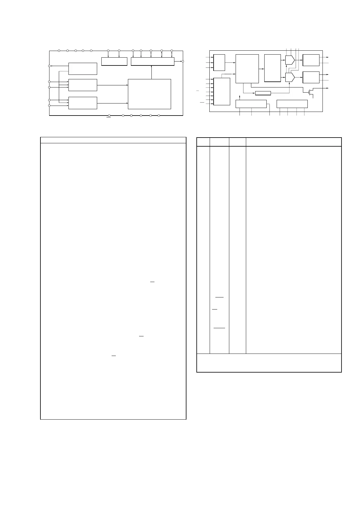
Serial
Input
I/F
Mode
Control
I/F
8X Oversampling
Digital Filter with
Function
Controller
Crystal/OSC
XTI
SCK
XTO CLKO V
CC1
AGND1 V
DD
DGND
Enhanced
Multi-level
Delta-Sigma
Modulator
V
OUT
L
V
CC2
L
V
CC2
R
AGND2L
AGND2L
EXTL
Open Drain
DAC
Low-pass
Filter
Low-pass
Filter
BPZ-Cont.
V
OUT
R
EXTR
ZERO
DAC
MC/DM1
ML/IIS
LRCIN
DIN
BCKIN
CS/IWO
MD/DM0
MODE
MUTE
RST
Power Supply
PIN NAME I/O DESCRIPTION
1 LRCIN IN Left and Right Clock Input. This clock is equal to
the sampling rate - f
S
.
(1)
2 DIN IN Serial Audio Data Input
(1)
3 BCKIN IN Bit Clock Input for Serial Audio Data.
(1)
4 CLKO OUT Buffered Output of Oscillator. Equivalent to
System Clock.
5 XTI IN Oscillator Input (External Clock Input)
6 XTO OUT Oscillator Output
7 DGND - Digital Ground
8V
DD
- Digital Power +5V
9V
CC
2R - Analog Power +5V
10 AGND2R - Analog Ground
11 EXTR OUT Rch, Common Pin of Analog Output Amp
12 NC - No Connection
13 V
OUT
R OUT Rch, Analog Voltage Output of Audio Signal
14 AGND1 - Analog Ground
15 V
CC
1 - Analog Power +5V
16 V
OUT
L OUT Lch, Analog Voltage Output of Audio Signal
17 NC - No Connection
18 EXTL OUT Lch, Common Pin of Analog Output Amp
19 AGND2L - Analog Ground
20 V
CC
2L - Analog Power +5V
21 ZERO OUT Zero Data Flag
22 RST IN Reset. When this pin is low, the DF and
modulators are held in reset.
(2)
23 CS/IWO IN Chip Select/Input Format Selection. When this
pin is low, the Mode Control is effective.
(3)
24 MODE IN
Mode Control Select. (H: Software, L: Hardware)
(2)
25 MUTE IN Mute Control
26 MD/DM0 IN Mode Control, DATA/De-emphasis Selection 1
(2)
27 MC/DM1 IN Mode Control, BCK/De-emphasis Selection 2
(2)
28 ML/I
2
S IN Mode Control, WDCK/Input Format Selection
(2)
NOTES: (1) Pins 1, 2, 3; Schmitt Trigger input. (2) Pins 22, 24, 25, 26, 27,
28; Schmitt Trigger input with pull-up resister. (3) Pin 23; Schmitt Trigger
input with pull-down resister.
Q401 : PCM1716
Voltage
Reference
Modulator
D S
Modulator
D S
Digital Decimation
Filter
Serial Output
Interface
Clock Divider
5 4 12 13 24 22 17 15 23 18 19 20
21
3
6
7
1
2
VREF
AINL+
AINL -
AINR+
AINR -
AGND VA VD DGND VB CMODE MCLK SMODE2 SCLK LRCK FSYNC
S DATA
SMODE1
PD HPFE TST1 TST2 TST3 TST4
16 9 8 10 11 14
Test pin Should be left floating. (Pull- down pin)
No. Pin Name I/O PIN / FUNCTION
1 AINR+
I
Right channel analog positive input pin
2 AINR-
I
Right channel analog negative input pin
3 VREF
O
Voltage Reference output pin (VA-2.6V)
Normally connected to VA with a 0.1uF ceramic capacitor in
parallel with a 10uF electrolytic capacitor.
4 VA Analog section Analog Power Supply, +5V
5 AGND Analog section Analog Ground
6 AlNL+
I
Left channel analog positive input pin
7 AINL-
I
Left channel analog negative input pin
8 TST1
Test pin Should be left floating. (Pull- down pin)
Test pin Should be left floating. (Pull- down pin)
Test pin Should be left floating. (Pull- down pin)
10 TST2
11 TST3
14 TST4
9 HPFE
I
High Pass Filter Enable pin (Pull- up pin)
"H": ON
"H": OFF
12 VD Digital section Digital Power Supply pin, +5V
13 DGND Digital section Digital Ground pin
16 PD
I
Power Down pin
"L" brings the device into power-down mode. Must be done
once after power-on.
17 MCLK I Master Clock input pin
CMODE="H" : 384fs
CMODE="L" : 256fs
18 SCLK I/O Serial Data Clock pin
Data is clocked out at the falling edge of SCLK.
Slave mode: 64fs clock is input usually.
Master mode: SCLK outputs a 64fs clock.
SCLK stays low during the power-down mode(PD="L").
19 LRCK I/O L/R Channel Clock Select pin
Slave mode: An fs clock is fed to this LRCK pin.
Master mode: LRCK output an fs clock.
LRCK goes "H" at SMODE2="L" and "L" at SMODE2="H"
during reset when SMODE1 "H".
20 FSYNC I/O Frame Synchronization Signal pin
S!ave mode: When "H", data bits are clocked out on SDATA.
As I
2
S slave mode ignores FSYNC It should hold "L" or
"H".
Master mode: FSYNC outputs 2fs clock.
Stay low during the power-down mode(PD="L") .
21 SDATA O Serial Data Output pin
Data are output with MSB first, in 2's complement format.
After 20 bits are output it turns to "L". It also remains "L" at a
power- down mode(PD="L").
22 CMODE I Master Clock Selection pin
"L": MCLK=256fs
"H": MCLK=384fs
23 SMODE1 I Serial Interface Mode Select pin
15 SMODE2 I Defines the directions of LRCK, SCLK and FSYNC pins and
Output Data Format. SMODE2 is pull- down pin.
SMODE1 SMODE2 MODE LRCK
L L Slave mode: MSB justified : H/L
H L Master mode Similar to I
2
S : H/L
L H Slave mode: I
2
S : L/H
H H Master mode: I
2
S : L/H
24 VB
Substrate Power Supply, +5V
Q351 : AK5351
 Loading...