7I76 4
CONNECTORS
P1 HOST INTERFACE CONNECTOR
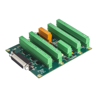
P1 is the DB25F connector on the 7I76 that connects to the FPGA card. Actual pin
functions depend on FPGA configuration but signal directions must be observed.
DB25 PIN GPIO FUNCT DIR DB25 PIN GPIO FUNC DIR
1 IO0 DIR0 OUT 14 IO1 STEP0 OUT
2 IO2 DIR1 OUT 15 IO3 STEP1 OUT
3 IO4 DIR2 OUT 16 IO5 STEP2 OUT
4 IO6 DIR3 OUT 17 IO7 STEP3 OUT
5 IO8 DIR4 OUT 18 GND
6 IO9 STEP4 OUT 19 GND
7 IO10 SS0TX OUT 20 GND
8 IO11 SS0RX IN 21 GND
9 IO12 SS1TX OUT 22 GND or 5V
10 IO13 SS1RX IN 23 GND or 5V
11 IO14 ENCI IN 24 GND or 5V
12 IO15 ENCB IN 25 GND or 5V
13 IO16 ENCA IN
Notes
1. If jumper W2 is is the left hand position, pins 22 through 25 are 5V, if W2 is in the right
hand position, Pins 22 through 25 are GND.
2. GPIO pins are for first FPGA connector, next connector series begins at GPIO17
3. Signal directions are relative to FPGA card, that is, an ‘OUT’ signal is an output from the
FPGA card that drives the 7I76. Conversely an ‘IN’ signal is a FPGA input that is driven
by the 7I76.