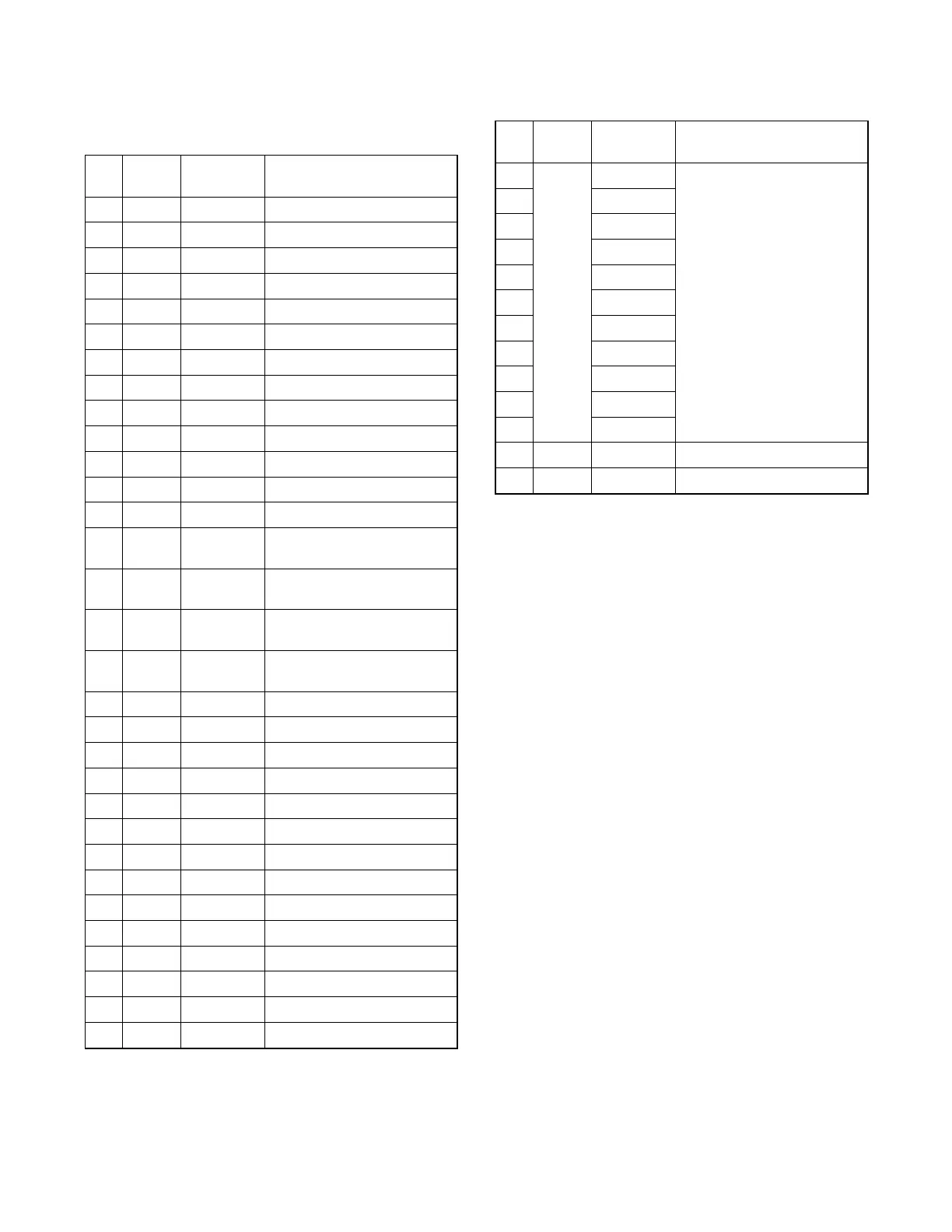
IC PIN FUNCTION DESCRIPTIONS
IC2003 ( PT6315 )
Pin
No.
In/
Out
Signal
Name
Function
1 - N.U. Not Used
2 - N.U. Not Used
3 - N.U. Not Used
4 - N.U. Not Used
5 In OSC Oscillator Input
6 Out DOUT Serial Data Output
7 In DIN Serial Data Input
8 In CLK Clock Input
9 In STB Serial Interface Strobe
10 In K1 Key Data 1 Input
11 In K2 Key Data 2 Input
12 - VSS GND
13 - VDD Power Supply
14 Out a / KEY-1
Segment Output
/ Key Souce-1
15 Out b / Key-2
Segment Output
/ Key Souce-2
16 Out c / Key-3
Segment Output
/ Key Souce-3
17 Out d / Key-4
Segment Output
/ Key Souce-4
18 OUT e Display Segment
19 OUT f Display Segment
20 OUT g Display Segment
21 OUT h Display Segment
22 OUT i Display Segment
23 OUT j Display Segment
24 - N.U. Not Used
25 - N.U. Not Used
26 - N.U. Not Used
27 - N.U. Not Used
28 - N.U. Not Used
29 - N.U. Not Used
30 - VEE Pull Down Level
31 - N.U. Not Used
Pin
No.
In/
Out
Signal
Name
Function
32
OUT
11G
Grid Output
33 10G
34 9G
35 8G
36 7G
37 6G
38 5G
39 4G
40 3G
41 2G
42 1G
43 - VDD Power Supply
44 - VSS GND
1-11-1 E5540PIN