Chapter 1: 2-8 Notes For All Schematics and Circuit Boards
6881091C63-A
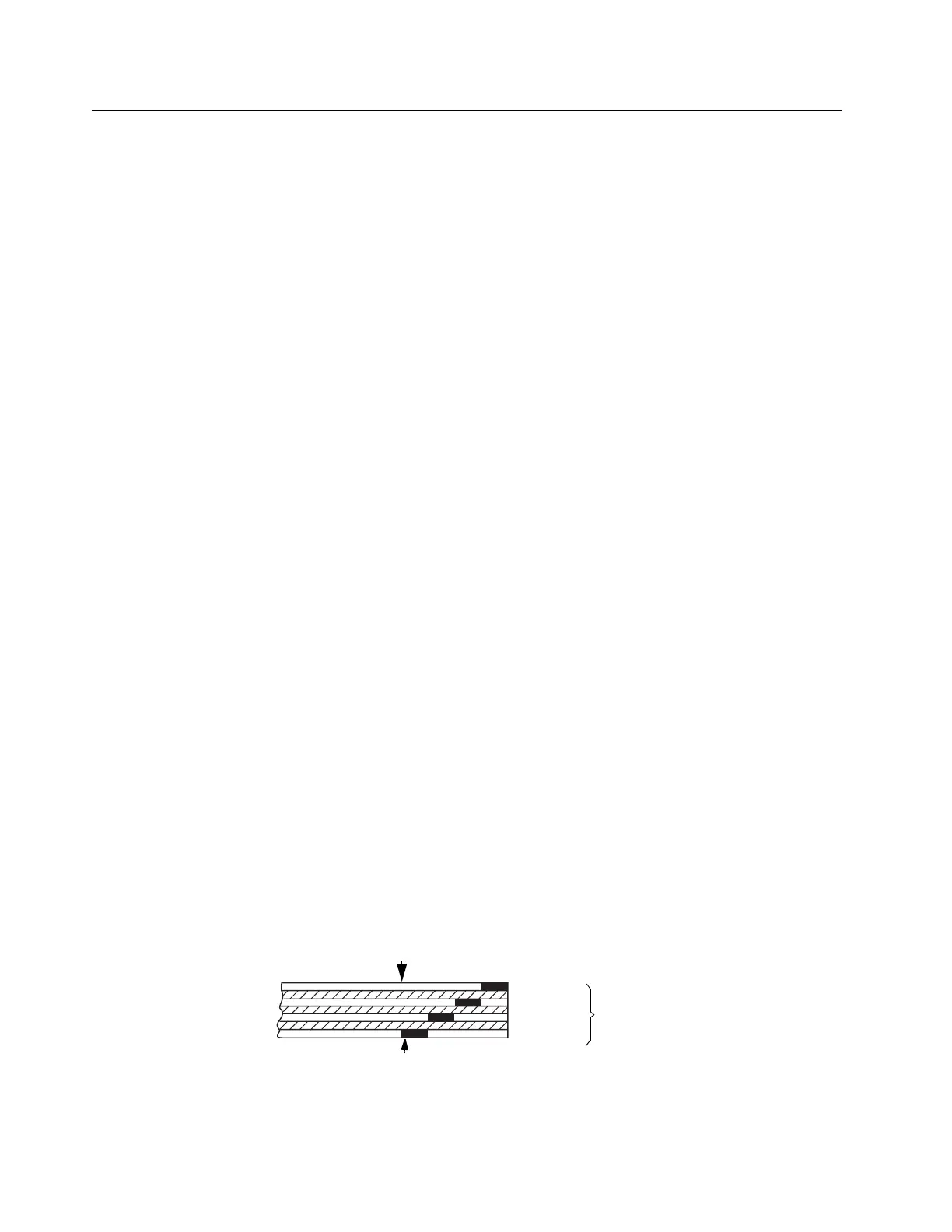
Four-layer circuit board detail, viewing copper steps in proper layer sequence
SPKR+ Positive Audio PA Speaker Output
SQ DET Squelch Detect Signal
SYN µP Clock Signal
TEMP SENSE Temperature Sense Line for LCD
TEMPSENSE Temperature Sense Line from PA to µP
TRB TX/RX VCO Switch Signal
TX AUD RTN Option Board Output to Transmit Audio Path
TX AUD SND Microphone Audio to Option Board
TXINJ RF Signal from the VCO into the Transmitter PA
U DRIVER Supply Voltage for PA Driver
U PREDRIVER Supply Voltage for PA Pre-driver
UNSW 5V Permanent 5V Supply
URX SND Filtered Audio Signal to Option Board
VAG 2.5V Reference Voltage for Analog Circuitry
VCOBIAS 1 Switch Signal from Synthesizer
VCOBIAS 2 Switch Signal from Synthesizer
VCOMOD Modulation Signal into VCO
VCTRL VCO Frequency Control Voltage
VDDA Regulated 5V for Digital Circuitry in RF Section
VOLTAGE SENSE Voltage Sense Line from LCD
VOLUME Volume Pot Output
VOX Voice Operated Transmit Level
VPP Boot Mode Select
VS AUDIOSEL Switch Signal to Enable Option Board Audio
Output Signal
VS GAINSEL Voice Storage Gain Select Line
VS INT Voice Storage Interrupt Line
VS MIC Voice Storage Audio Signal into Microphone Path
VS RAC Voice Storage Row Address Clock Signal
VSF Voltage Super Filtered (5V)
VSTBY 5V Supply for µP when the Radio is switched off
LAYER 1 (L1)
LAYER 2 (L2)
LAYER 3 (L3)
LAYER 4 (L4)
INNER LAYERS
SIDE 1
SIDE 2
 Loading...