Notes For All Schematics and Circuit Boards 2-5
5.0 Notes For All Schematics and Circuit Boards
* Component is frequency sensitive. Refer to the Electrical Parts List for value and usage.
1. Unless otherwise stated, resistances are in Ohms (k = 1000), and capacitances are in picofarads
(pF) or microfarads (µF).
2. DC voltages are measured from point indicated to chassis ground using a Motorola DC
multimeter or equivalent. Transmitter measurements should be made with a 1.2 µF choke in
series with the voltage probe to prevent circuit loading.
3. Interconnect Tie Point Legend:
UNSWB+ = Unswitch Battery Voltage (7.5V)
SWB+ = Switch Battery Voltage (7.5V)
R5 = Receiver Five Volts
CLK = Clock
Vdda = Regulated 3.3 Volts (for analog)
Vddd = Regulated 3.3 Volts (for digital)
CSX = Chip Select Line (not for LVZIF)
SYN = Synthesizer
DACRX = Digital to Analog Voltage (For Receiver Front End Filter)
VSF = Voltage Super Filtered (5 volts)
VR = Voltage Regulator
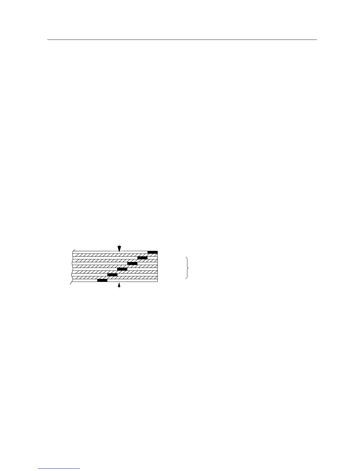
6-LAYER CIRCUIT BOARD DETAIL VIEWING
COPPER STEPS IN PROPER LAYER SEQUENCE
LAYER 1 (L1)
LAYER 2 (L2)
LAYER 3 (L3)
LAYER 4 (L4)
LAYER 5 (L5)
LAYER 6 (L6)
INNER LAYERS
SIDE 1
SIDE 2

 Loading...