2-8 THEORY OF OPERATION
4.3 Automatic Gain Control (AGC)
(
Refer to the Receiver Front End and Receiver Back End schematic diagrams
)
The front end automatic gain control circuit provides automatic reduction of gain of the front end RF
amplifier via feedback. This prevents overloading of backend circuits and is achieved by drawing
some of the output power from the RF amplifier output. At high radio frequencies, capacitor C3327
provides the low impedance path to ground for this purpose. CR3302 is a pin diode used for
switching the path on or off. A certain amount of forward biasing current is needed to turn the pin
diode on. Transistor Q3301 provides this current.
Radio signal strength indicator, RSSI, a voltage signal, is used to drive Q3301 to saturation i.e.
turned on. RSSI is produced by U3220 and is proportional to the gain of the RF amplifier and the
input power to the radio.
Resistors R3304 and R3305 are voltage dividers designed to turn on Q3301 at certain RSSI levels.
To turn on Q3301 the voltage across R3305 must be greater or equal to the voltage across R3324 +
Vbe. Capacitor C3209 is used to dampen any instability while the AGC is turning on. The current
flowing into the collector of Q3301, a high current gain NPN transistor, is drawn through the pin
diode to turn it on. Maximum current flowing through the pin is limited by resistors R3316, R3313,
R3306 and R3324. Feedback capacitor C3326 used to provide some stability to this high gain
stage.
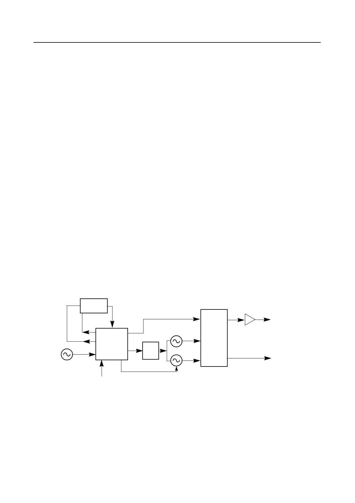
5.0 Frequency Generation Circuit
(
Refer to Figure 2-4 and the VHF Frequency Synthesizer schematic diagram
)
The Frequency Generation Circuit, shown in Figure 2-4, is composed of two main ICs, the
Fractional-N synthesizer (U3701), and the VCO/Buffer IC (U3801). Designed in conjunction to
maximize compatibility, the two ICs provide many of the functions that normally would require
additional circuits. The synthesizer block diagram illustrates the interconnect and support circuit
used in the region. Refer to the schematic for the reference designator.
Figure 2-4 VHF Frequency Generation Unit Block Diagram
The synthesizer is powered by regulated 5V and 3.3V which is provided from ICs U3711 and U3201
respectively. The 5V signal is supplied to pins 13 and 30 and the 3.3V signal is applied to pins 5, 20,
34 and 36 of U3701. The synthesizer in turn generates a superfiltered 5V which powers U3801.
Voltage
Multiplier
Synthesizer
U3701
Loop
Filter
VCOBIC
U3801
To
Mixer
To
PA Driver
VCP
Vmult1
Aux3
MOD Out
Modulating
Signal
Vmult2
Rx VCO Circuit
Tx VCO
TRB
16.8 MHz
Ref. Osc.
Rx Out
Tx Out
Circuit

 Loading...